PCB Design Best Practices
-
Verify Schematic Accuracy:
Before diving into PCB design, meticulously check the schematic diagram to ensure signal integrity and proper device connections.
-
Component Selection:
Carefully choose components, considering packaging variations that impact solder hole configurations.
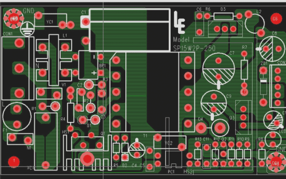
Essential Tips for Multi-layer PCB Design:
-
Board Shape, Size, and Layer Count:
Ensure the PCB shape aligns with the product’s structure for easy assembly and production efficiency. Opt for symmetrical layers in multiples of four for stability.
-
Component Positioning:
Place components logically to enhance PCB performance, especially crucial for high-frequency analog circuits.
-
Wire Layout and Area:
Distribute wiring based on circuit functions, with outer layers favoring more wiring on the soldering surface for maintenance and heat dissipation.
-
Wire Orientation and Width:
Separate power, ground, and signal layers to minimize interference, avoiding parallel lines to reduce coupling and interference.
-
Drilling and Pad Requirements:
Adhere to specific drilling sizes and pad configurations to ensure precision and reliability in your PCB design.
Proper insulation and adherence to design principles are vital in creating functional and durable printed circuit boards. For more detailed guidance on PCB design, consult industry experts and stay updated on the latest technological advancements.
PCB Design Best Practices
The key considerations for designing a printed circuit board (PCB) include:
- Component Hole Size and Pad Diameter: Match the hole diameter to the pin size, with a slight margin for assembly. Pad diameter should be at least the hole diameter plus 18 mils.
- Via Design: Via hole diameter should follow a ratio of ≤ 5:1 to the board thickness. The via pad diameter should be 12 mils larger than the via hole diameter.
- Power Supply and Ground Layers: Multi-layer boards need at least one power layer and one ground layer, with partitioned and isolated power layers.
- Safety Clearance: Maintain proper spacing according to electrical safety standards to avoid interference and board failure.
- Anti-Interference Measures: Enhance resistance to interference by strategic component placement and grounding.
- Outsourcing Guidelines: Accurately specify material choices, lamination order, and processing technology for outsourced PCB manufacturing.
Additional Considerations
Aside from the above requirements, factors like external connections, component placement, electromagnetic protection, and heat dissipation play a crucial role in PCB design. Pay special attention to selecting high-quality connectors for optimal performance.
I trust this updated information aligns with your expectations!