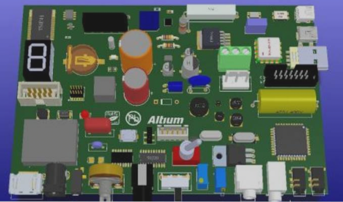
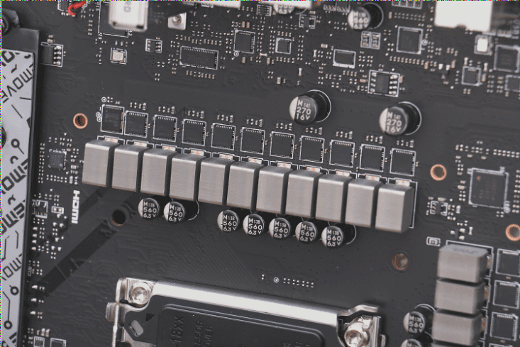
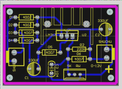
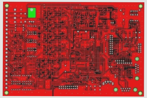
As we all know, SMT chip processing imposes specific requirements on PCB design. Only PCBs designed with appropriate specifications can fully leverage the capabilities of SMT chip equipment, enabling efficient PCBA processing.
**SMT Chip Processing Requirements for PCB Design**
The requirements of SMT patch processing for PCB design encompass shape, size, thickness, positioning holes, process edges, fiducial marks, and the board itself.
1. **PCB Shape**
PCBs are typically rectangular, with the optimal aspect ratios being 3:2 or 4:3. A larger aspect ratio can lead to warping and deformation. It is advisable to standardize PCB sizes as much as possible to streamline the processing and reduce costs.
2. **PCB Size**
Different SMT equipment has varying requirements for PCB dimensions. When designing a PCB, it is essential to consider the maximum and minimum mounting sizes specified by the SMT equipment. Typical dimensions range from 50*50 mm to 350*250 mm, with newer SMT machines accommodating larger sizes; for instance, Universal’s Genesis GX can handle PCBs up to 813*610 mm.

3. PCB Thickness
The thickness of the PCB should take into account the mechanical strength requirements and the component weight per unit area, typically ranging from 0.3 to 6mm. Commonly used PCB thickness is 1.6mm, while extra-large boards can reach 2mm. Microstrip boards for radio frequency applications generally measure between 0.8 and 1mm.
4. PCB Positioning Hole
Some SMT equipment, like placement machines, utilize hole positioning. To ensure accurate PCB fixation on the equipment fixture, positioning holes must be reserved. Different devices have varying requirements; typically, a pair of positioning holes is needed in the lower left and lower right corners of the PCB, with a hole diameter of Φ4mm (Φ3mm or Φ5mm are also options). The hole walls should not be metalized, and one hole can be designed as an oval for quicker positioning. The distance between the main positioning hole and the PCB edges should be 5mm each, while the adjustment hole should maintain a 5mm distance from the bottom of the PCB. No SMD components are allowed within a 5mm radius of the positioning holes.
5. PCB Process Side
During the SMT production process, the PCB is moved via track transmission. To ensure reliable fixation, a 5mm space is generally reserved on the long side of the transmission track to facilitate equipment clamping, with no devices allowed in this area. If reserving space is not feasible, a process edge must be added. For plug-in products subjected to wave soldering, a 3mm margin is typically required on the short side to accommodate the tin strip.
6. PCB Fiducial Mark (Fiducial Mark)
The fiducial mark, also known as a reference point, serves as a common measurable point throughout the SMT assembly process, ensuring accurate positioning of circuit patterns for each device. Hence, fiducial marks are crucial in SMT production and are categorized into whole board marks, jigsaw marks, and partial recognition marks (foot spacing ≤0.5mm). Generally, the mark point consists of metal copper foil with a diameter of 1.0mm, surrounded by a contrasting open area of 3mm. There should be a clear color distinction between the copper foil and the surrounding area, with no silk screen, pad, or V-Cut allowed within a Φ3mm radius.
7. PCB Board Design
General principle: When the PCB size is less than 50mm x 50mm, assembly is required. For PCBs under 160mm x 120mm, panel design is recommended to achieve an ideal size for plug-in and soldering, enhancing production efficiency and equipment utilization. However, the size of jigsaw puzzles should not be excessively large and must meet equipment requirements. V-shaped grooves, stamp holes, or punching grooves can be used between panels, with the same board employing only one splitting method. For double-sided SMD boards assembled across the entire surface, yin and yang imposition design can be adopted, allowing the use of a single stencil to save programming time and enhance production efficiency. Larger and heavier devices must adhere to the following restrictions: A=device weight/contact area between pins and pads.
SMT chip processing
The above outlines the requirements for SMT chip processing in PCB design.


