1. What is PCB sample production?
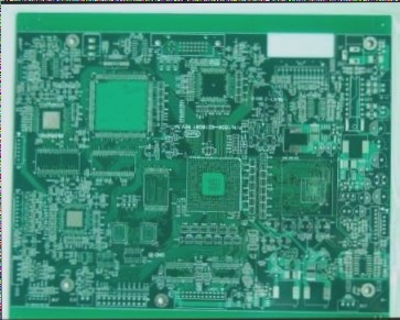
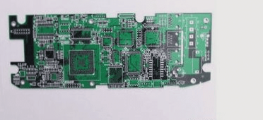
2. PCB sample production refers to the preliminary manufacturing of PCBs prior to mass production. The primary purpose is for electronic engineers to design circuits and complete the PCB fabrication process, followed by small-batch trial production at PCB factories—this is known as PCB sample production.
3. Additionally, PCB sample production typically involves sending electronic products to PCB manufacturers for trial runs after engineers finalize the PCB layout design and processing.
4. The rapid pace of electronic product updates drives an increasing demand for PCB sample production, which in turn expands its market share. As technological requirements for electronic products intensify, the speed of updates accelerates, resulting in a rise in multi-layer PCB sample production.

Who are the users of PCB sample production?
Primarily electronic engineers, along with academic researchers, research institutions, and various student groups.
How to select the appropriate PCB sample manufacturer
Choosing the right PCB sample manufacturer involves several key factors:
1. Larger companies typically offer more stable capabilities and standardized management practices.
2. Opt for manufacturers with comprehensive support facilities and reliable delivery schedules.
3. Select a company known for its strong reputation, quality service, and positive corporate culture.
What relevant parameters and instructions should be provided for PCB sample making?
Typically, PCB boards need processing by the manufacturer. After sample creation, technicians will solder components, assemble them into enclosures, and package the final product. What specific parameters and instructions are required for PCB sample fabrication?
Provide PCB sample preparation requirements
Data: First, clarify the data needed for PCB production. Currently, FR4 is the most common material, primarily consisting of epoxy resin and fiberglass cloth.
Layer: Describe your PCB (Each layer produced differs, affecting both cost and the sample production process, which is generally similar.)
Color of solder mask: Various colors are available, usually selected based on company preferences, with green being the standard.
Silk screen color: This refers to the color of the silk screen text and borders on the printed circuit board, typically white.
Copper thickness: Copper thickness is usually calculated based on the current requirements of the PCB circuit. Thicker copper is generally preferable, though it increases costs, necessitating a reasonable compromise.
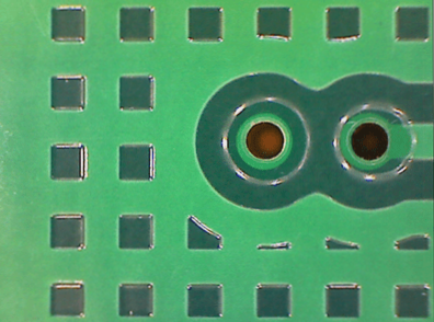
Whether the vias are covered with solder mask: The solder mask serves to insulate the vias, or, if desired, to leave them uninsulated.
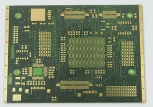
Surface coating: Options include tin plating and gold plating.
Quantity: Clearly specify the number of PCBs to be produced.
Additionally, Gerber files or PCB files should be provided. WellCircuits produces high-quality PCB samples tailored to customer specifications and supports high-standard mass PCB manufacturing.
2. PCB sample production refers to the preliminary manufacturing of PCBs prior to mass production. The primary purpose is for electronic engineers to design circuits and complete the PCB fabrication process, followed by small-batch trial production at PCB factories—this is known as PCB sample production.
3. Additionally, PCB sample production typically involves sending electronic products to PCB manufacturers for trial runs after engineers finalize the PCB layout design and processing.
4. The rapid pace of electronic product updates drives an increasing demand for PCB sample production, which in turn expands its market share. As technological requirements for electronic products intensify, the speed of updates accelerates, resulting in a rise in multi-layer PCB sample production.

Who are the users of PCB sample production?
Primarily electronic engineers, along with academic researchers, research institutions, and various student groups.
How to select the appropriate PCB sample manufacturer
Choosing the right PCB sample manufacturer involves several key factors:
1. Larger companies typically offer more stable capabilities and standardized management practices.
2. Opt for manufacturers with comprehensive support facilities and reliable delivery schedules.
3. Select a company known for its strong reputation, quality service, and positive corporate culture.
What relevant parameters and instructions should be provided for PCB sample making?
Typically, PCB boards need processing by the manufacturer. After sample creation, technicians will solder components, assemble them into enclosures, and package the final product. What specific parameters and instructions are required for PCB sample fabrication?
Provide PCB sample preparation requirements
Data: First, clarify the data needed for PCB production. Currently, FR4 is the most common material, primarily consisting of epoxy resin and fiberglass cloth.
Layer: Describe your PCB (Each layer produced differs, affecting both cost and the sample production process, which is generally similar.)
Color of solder mask: Various colors are available, usually selected based on company preferences, with green being the standard.
Silk screen color: This refers to the color of the silk screen text and borders on the printed circuit board, typically white.
Copper thickness: Copper thickness is usually calculated based on the current requirements of the PCB circuit. Thicker copper is generally preferable, though it increases costs, necessitating a reasonable compromise.
Whether the vias are covered with solder mask: The solder mask serves to insulate the vias, or, if desired, to leave them uninsulated.
Surface coating: Options include tin plating and gold plating.
Quantity: Clearly specify the number of PCBs to be produced.
Additionally, Gerber files or PCB files should be provided. WellCircuits produces high-quality PCB samples tailored to customer specifications and supports high-standard mass PCB manufacturing.


