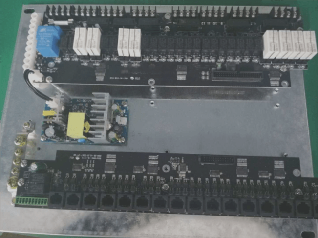
The improvement of PCB board process detection directly impacts the actual capabilities and long-term development of electronic products in domestic and global electronics industries and other sectors. As PCB technology advances, boards exhibit three main trends: narrower traces, smaller and increased trace spacing, and more pronounced height variations. These trends have notably accelerated over the past five years.
However, the development of PCB board industry instruments lags behind both domestically and internationally. This lag primarily stems from limitations in light source technology development. Inadequate light sources hinder effective illumination and information extraction for target objects, thereby severely restricting backend measurement technologies such as image processing algorithms and precision mechanical positioning.
In response,

1. Basic theory
1.1 Challenges in Designing Thick and Dense PCB Light Sources
In the PCB industry’s evolution, trends toward finer lines, smaller spacings, higher densities, and more pronounced height variations pose significant challenges. This paper focuses on thick dense boards, epitomizing these trends. Figure 1(a) illustrates a common light source on a PCB with wide spacing and thinness, while Figure 1(b) shows the same light source on a PCB with narrow spacing and thickness. A wide-spaced, thin board allows light to illuminate the substrate, bottom, and top lines effectively, enhancing contrast and aiding visual assessment. However, dense boards hinder light due to narrow angles, resulting in poor contrast and brightness between lines and substrates, complicating subsequent image-based measurements. This underscores the inadequacy of conventional light sources for thick dense boards.
1.2 Adaptive Ring Light Source Principle Based on Fixed-Angle Design
To address these challenges, a stable solution is needed that maintains accuracy in thick dense PCB illumination. This necessitates selecting optimal incident angles and configuring ring light sources tailored to these geometrical and optical characteristics. This paper proposes an adaptive ring light source with a fixed-angle design comprising a ring shell, circuit board, LED, and diffuser plate. A flexible circuit board with series and parallel lines powers LEDs, which emit directional light beneficial for highlighting specific areas. However, to mitigate pixel interference and ensure uniform brightness, a diffuser plate is employed.
2. Experimental Results and Discussion
2.1 Artifacts from Ordinary Light Source Illumination
Images captured using conventional light sources exhibit significant edge deviation from actual cross-sections. At 2X magnification, where each pixel corresponds to 1.61 μm on the object surface, false edges cause deviations exceeding 3 pixels in line width assessments. This erroneous edge effect stems from inadequate illumination angles of ordinary light sources, resulting in substrate and lower line widths appearing similar in brightness and color. Such deviations, not factored into standard measurements, introduce systematic errors in measured values, obscuring genuine circuit characteristics.
2.2 Impact of Geometric Features on Light Source Design
Given line height-to-spacing ratios around 1:2 (equating to a 27° angle), effective inspection of dense PCBs demands significantly wider light incident angles than those typical of common light sources. Achieving clear, contrasted images necessitates optimizing light angles to suit substrate and circuit optics.
2.3 Design of Fixed-Angle Adaptive Ring Light Source
Considering these factors, this study designs a specialized ring light source tailored for dense PCBs. Direct comparisons with standard light sources reveal stark contrasts in image quality. Conventional sources struggle with brightness uniformity due to blockages by dense lines, failing to effectively record PCB circuit details and leading to inaccuracies in line width analysis. Conversely, the proposed adaptive light source ensures uniformity and sharpness, effectively illuminating substrates, circuit transitions, and surfaces with stepped brightness gradients. Such enhancements are pivotal for precise testing and facilitate targeted information extraction for image processing.
3. Conclusion
To tackle the limitations of conventional light sources in dense PCB inspection, this study delves into pseudo-image errors from low-angle illumination and discusses how geometric and optical characteristics influence light source design. By introducing a purpose-built, fixed-angle ring light source, this research not only addresses existing challenges but also enhances front-end system illumination and precise information extraction. The improved image uniformity and contrast achieved significantly benefit back-end processing and information extraction, underscoring its potential for widespread adoption in PCB inspection equipment, particularly line width inspection machines.
However, the development of PCB board industry instruments lags behind both domestically and internationally. This lag primarily stems from limitations in light source technology development. Inadequate light sources hinder effective illumination and information extraction for target objects, thereby severely restricting backend measurement technologies such as image processing algorithms and precision mechanical positioning.
In response,

1. Basic theory
1.1 Challenges in Designing Thick and Dense PCB Light Sources
In the PCB industry’s evolution, trends toward finer lines, smaller spacings, higher densities, and more pronounced height variations pose significant challenges. This paper focuses on thick dense boards, epitomizing these trends. Figure 1(a) illustrates a common light source on a PCB with wide spacing and thinness, while Figure 1(b) shows the same light source on a PCB with narrow spacing and thickness. A wide-spaced, thin board allows light to illuminate the substrate, bottom, and top lines effectively, enhancing contrast and aiding visual assessment. However, dense boards hinder light due to narrow angles, resulting in poor contrast and brightness between lines and substrates, complicating subsequent image-based measurements. This underscores the inadequacy of conventional light sources for thick dense boards.
1.2 Adaptive Ring Light Source Principle Based on Fixed-Angle Design
To address these challenges, a stable solution is needed that maintains accuracy in thick dense PCB illumination. This necessitates selecting optimal incident angles and configuring ring light sources tailored to these geometrical and optical characteristics. This paper proposes an adaptive ring light source with a fixed-angle design comprising a ring shell, circuit board, LED, and diffuser plate. A flexible circuit board with series and parallel lines powers LEDs, which emit directional light beneficial for highlighting specific areas. However, to mitigate pixel interference and ensure uniform brightness, a diffuser plate is employed.
2. Experimental Results and Discussion
2.1 Artifacts from Ordinary Light Source Illumination
Images captured using conventional light sources exhibit significant edge deviation from actual cross-sections. At 2X magnification, where each pixel corresponds to 1.61 μm on the object surface, false edges cause deviations exceeding 3 pixels in line width assessments. This erroneous edge effect stems from inadequate illumination angles of ordinary light sources, resulting in substrate and lower line widths appearing similar in brightness and color. Such deviations, not factored into standard measurements, introduce systematic errors in measured values, obscuring genuine circuit characteristics.
2.2 Impact of Geometric Features on Light Source Design
Given line height-to-spacing ratios around 1:2 (equating to a 27° angle), effective inspection of dense PCBs demands significantly wider light incident angles than those typical of common light sources. Achieving clear, contrasted images necessitates optimizing light angles to suit substrate and circuit optics.
2.3 Design of Fixed-Angle Adaptive Ring Light Source
Considering these factors, this study designs a specialized ring light source tailored for dense PCBs. Direct comparisons with standard light sources reveal stark contrasts in image quality. Conventional sources struggle with brightness uniformity due to blockages by dense lines, failing to effectively record PCB circuit details and leading to inaccuracies in line width analysis. Conversely, the proposed adaptive light source ensures uniformity and sharpness, effectively illuminating substrates, circuit transitions, and surfaces with stepped brightness gradients. Such enhancements are pivotal for precise testing and facilitate targeted information extraction for image processing.
3. Conclusion
To tackle the limitations of conventional light sources in dense PCB inspection, this study delves into pseudo-image errors from low-angle illumination and discusses how geometric and optical characteristics influence light source design. By introducing a purpose-built, fixed-angle ring light source, this research not only addresses existing challenges but also enhances front-end system illumination and precise information extraction. The improved image uniformity and contrast achieved significantly benefit back-end processing and information extraction, underscoring its potential for widespread adoption in PCB inspection equipment, particularly line width inspection machines.


