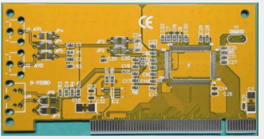
1. If you find that the PCB design experience gained during the previous low-speed era no longer seems applicable, and a design that worked fine before now malfunctions, then congratulations—you’ve encountered the most fundamental issue in PCB hardware design: Signal integrity.
2. It’s fortunate that you’re facing this challenge now. During the low-speed era, signal rise times typically increased by a few nanoseconds when the signal levels changed, and the interconnections between devices had little impact on circuit functionality. Signal integrity was not a concern.
3. However, in today’s high-speed era, with IC switching speeds reaching the picosecond level, almost every design, regardless of signal period, faces signal integrity challenges. Additionally, the push for lower power consumption has led to a continuous reduction in core voltages, with 1.2V core voltage now being quite common.
1. Therefore, the noise tolerance of the system tends to decrease, which makes the signal integrity issues more pronounced. Broadly speaking, signal integrity refers to all the problems arising from interconnections in circuit design. It primarily focuses on how the electrical characteristics of these interconnections interact with the voltage and current waveforms of digital signals, and how this interaction impacts the overall performance of the product.
2. These issues manifest in various ways, including timing errors, signal ringing, signal reflection, near-end and far-end crosstalk, switching noise, non-monotonicity, ground bounce, power bounce, attenuation, capacitive loading, electromagnetic radiation, and electromagnetic interference, among others. The core of the signal integrity problem lies in the reduction of the signal rise time.
3. Even if the wiring topology remains unchanged, using an IC with a slower rise time may push the existing design into a critical state or cause it to fail entirely.
4. Below are some common signal integrity problems: **Waveform distortion caused by signal reflection.** This appears as ringing. If you measure signals from a circuit board you’ve designed, such as clock outputs or high-speed data lines, and observe such waveforms, then you are encountering a signal integrity issue. Many hardware engineers connect a small resistor to the clock output signal, but often they can’t explain why. They may say it’s a feature of mature designs. While you may know, many engineers—some with three to four years of experience—don’t fully understand the function of this resistor. It may be surprising, but it’s true. The purpose of this small resistor is to address signal reflection. Increasing the resistance eliminates the ringing, but the rising edge of the signal may no longer be as steep. This method is called impedance matching. As shown on the right, impedance matching is a critical factor in signal integrity problems.
5. **Crosstalk**: If you observe carefully, you may notice that sometimes a signal line, even though it doesn’t have an output function, still shows a small, regular waveform during measurement, as if a signal is being output. At this point, you can measure the adjacent signal line to see if it exhibits a similar pattern. If the two signal lines are very close together, this is often the case. This phenomenon is called crosstalk. The waveform on the affected signal line doesn’t always resemble the adjacent signal’s waveform, nor does it necessarily follow a clear pattern; it often appears as noise. Crosstalk remains a major challenge in today’s high-density circuit boards, where small wiring spaces force signals to be placed close together. You can control crosstalk, but you can’t fully eliminate it—it’s an issue you must manage rather than avoid.
6. For signal lines affected by crosstalk, the interference from adjacent signals acts like noise. The extent of crosstalk is influenced by many factors on the PCB, not just the distance between the signal lines. While distance is the easiest factor to control and the most common solution for crosstalk, it’s not the only one. Many PCB engineers misunderstand this.
7. **Track collapse**: Noise is not limited to the signal network—it also affects the power distribution system. We know that the current flowing through the path between the power supply and ground inevitably encounters impedance, unless the entire circuit board is made from superconducting materials. As the current changes, a voltage drop occurs, which means the voltage reaching the chip’s power pin will be reduced, sometimes significantly, causing what is known as rail collapse. Track collapse can sometimes result in severe issues and may impact the functionality of the entire board. As high-performance processors integrate more gates, increase switching speeds, and consume more current over shorter times, the noise tolerance of the system becomes smaller and smaller. The stringent requirements of high-performance processors on the power system, combined with the difficulty of constructing a low-impedance power distribution system, make noise control increasingly challenging.
8. You might have noticed the recurring importance of impedance, and understanding impedance is key to addressing PCB signal integrity issues.