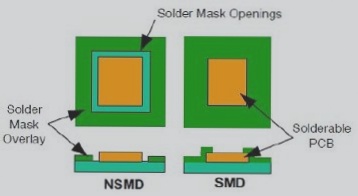
The Importance of PCB Reflow in Digital Circuits
In digital PCB schematics, signal propagation occurs through the movement of electrons, highlighting the significance of current flow. While voltage-mode devices are commonly used, understanding the path of the circuit and the flow of current is crucial.
Key Points to Note:
- Signals are transmitted by electric current, emphasizing the loop flow of electrons.
- High-frequency signal transmission involves charging dielectric capacitors between transmission lines and the DC layer.
Impact of PCB Reflow on Signal Return Paths
Digital circuits rely on ground and power planes for signal return paths, with different requirements for high and low-frequency signals. It is essential to consider the impedance and inductance of the return paths for optimal signal integrity.
Key Considerations:
- Ground and power planes play a vital role in facilitating signal return paths.
- Understanding the flow of current from the driver to the receiver is crucial for minimizing noise frequencies.
- Implementing measures to control return paths helps reduce interference and optimize signal integrity.
Additional Insights:
When dealing with multiple digital signals on a PCB, synchronous switching noise and ground bounce can impact signal quality. By analyzing the switching behavior of digital chips and controlling return paths, we can minimize noise and enhance overall performance.
Impact of PCB Layout on Signal Integrity at High Frequencies
At high frequencies, the layout of a Printed Circuit Board (PCB) plays a crucial role in maintaining signal integrity. One key issue to address is the “ground return” problem, particularly significant for high-frequency signals.
Ground Return Problem
When there is a surge in current on the signal line, such as from S1 to R1, the rapidly changing magnetic field induces a reverse current in nearby conductors. To mitigate this, a continuous third-layer ground plane can help. The return current flows through this ground plane, minimizing energy radiation and reducing external signal coupling.
Powering the Chip
High-frequency signals experience rapid changes in level and current, requiring minimal energy. Decoupling capacitors, like C1, play a crucial role in providing power to the chip. With a responsive and low Equivalent Series Resistance (ESR) capacitor, the signal loop’s paths on the TOP and GND layers become negligible.
Current Path in PCB
In a well-designed PCB environment, the current path flows from the positive terminal of C1 through various components and layers, eventually returning to the negative terminal of the capacitor. Proper design is crucial to prevent external interference and crosstalk, especially in clock signals with parallel data lines.
Minimizing Crosstalk
Ensuring proper matching of clock lines and data lines is essential to avoid significant disruptions caused by crosstalk. The intensity of crosstalk is not solely dependent on the interference source’s high and low levels but rather on the rate of current change within the source.
- If you have any inquiries about PCB design, feel free to reach out to us at info@wellcircuits.com