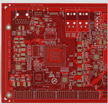
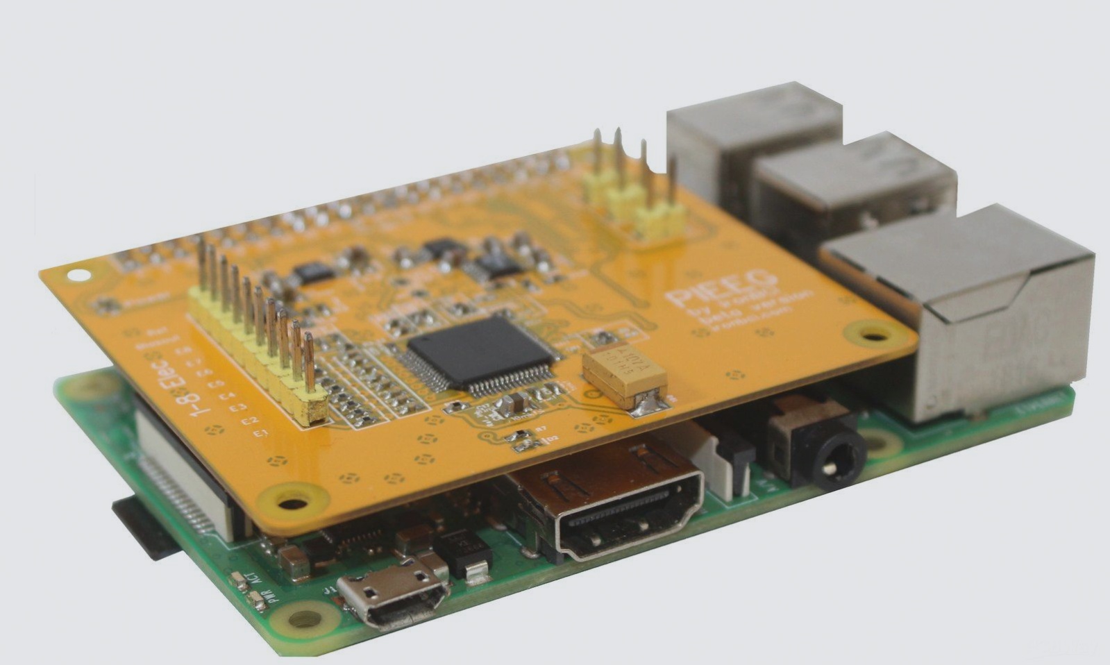
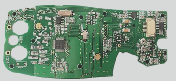
PCB Boards Overview
- PCB boards come in single-layer, double-layer, and multi-layer options.
- Single-layer PCBs have components on one side and wiring on the other.
- Double-layer PCBs are two single-layer boards stacked together.
- Multi-layer PCBs have multiple layers with vias connecting them.
Types of PCB Layers
- Single-layer PCB: Components on one side, wiring on the other.
- Double-layer PCB: Components and wiring on both sides.
- Multi-layer PCB: More layers for complex circuits, with ground and power layers.
Manufacturing Process
- Complex manufacturing process involving rolling, cutting, etching, and more.
- Layers include component surface, power layer, ground layer, and solder pressure layer.
- Quality checks ensure proper bonding and avoid short circuits.
Copper Wiring Process
The copper wiring process involves transferring the working film onto the metal conductor using various methods:
- Negative film transfer method: Applies copper foil and removes excess material.
- Positive photoresist method: Uses sensitizer and UV light to create wiring patterns.
- Etching: Removes exposed copper to form the final wiring layout.
PCB Design Best Practices
1. Trace Width and Current Handling
- Minimum trace width should be at least 0.2mm (8mil).
- For high-density PCBs, aim for a trace pitch and width of around 0.3mm (12mil).
- With a copper foil thickness of approximately 50µm, the trace width should range from 1–1.5mm (60mil) to support currents up to 2A.
- Commonly, 80mil traces are used, especially in applications involving microprocessors.
2. High-Speed PCB Frequency Considerations
- A signal is deemed high-speed when its rise/fall time is less than 3–6 times the signal’s transmission time.
- For digital circuits, focus on the steepness of the signal edge, particularly the rise and fall times.
- Referencing *High-Speed Digital Design*, a signal is high-speed if it rises from 10% to 90% of its maximum amplitude in less than six times the trace delay.
- Even an 8kHz square wave can be high-speed if the signal edges are sharp, requiring application of transmission line theory during routing.
3. Power and Ground Layout Tips
- Keep power traces short and direct, ideally in a tree structure rather than a loop.
- Ground loop issues in digital circuits typically result in minimal voltage drops, usually not affecting circuit operation adversely.
- Utilizing a 2Gsps oscilloscope to measure ground currents reveals insights into pulse width and potential differences between ground points.
- Separating analog ground loops on the PCB can mitigate frequency interference from space and improve circuit performance.
- Addressing humming in amplifier outputs may involve cutting ground loops, as observed in high-end “Hi-Fi” devices.
If you require PCB manufacturing services or have any inquiries, feel free to contact me.