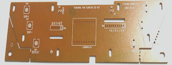
All of these characteristics require proficiency in the application of mathematics, not only in the design of the circuit board but also in the installation of components, including voltage, current, resistance, time constant, impedance, impedance matching, logic, and creativity regulation, and an innate understanding of the interaction between these interrelated factors.
Radio frequency (RF) devices are currently one of the most exciting applications in the field of electronic design. Any emerging technology used in smartphones, sensors, robotics, and security will require these complex high-frequency circuit boards. But, as we all know, for engineers like you who have to design them, it’s even more complicated and can be quite the headache!
RF PCB is one of the fastest-growing sectors in PCB manufacturing. With the proliferation of IoT sensors, wireless electronics, and smartphones, it’s easy to understand why. But how do you know if you’re using an RF PCB? The PCB industry considers any circuit board operating above 100MHz to be an RF PCB. Anything around 2GHz is a microwave PCB. This application note is designed for the design and layout of RF printed circuit boards. These are highly complex devices that can include up to 60 layers of configuration of digital, analog, and RF components! Here is a small sample of some of the guiding principles you can find:
1. Use VIAs to make transmission line layer changes:
Does your RF layout require you to move transmission lines between tiers? It is recommended to use at least two through-holes per conversion point to minimize the through-hole inductance load. The width of these transition holes should match the width of the transmission line. These holes are effectively used to reduce the transition inductance by 50%.
2. Correctly add line bend and corner compensation:
If your transmission line needs to change direction, then you will need to use a bending radius at least 3 times the width of the center conductor. This will ensure that the impedance remains stable as the current passes through the bend. If you cannot gently bend the bend and end up with a right-angle trace, then you will need to use the inclined bevel cut shown below. This helps to reduce impedance fluctuations, which can be found using Douville and James’ formulas.
3. Biasing and grounding routing:
The return current path of the system bias layer should always be considered in the RF design. Adding a signal layer between the offset and the grounded layer creates a larger return path, as shown below, resulting in noise coupling at the signal layer. For optimal layout, make sure there is no signal layer between the offset and the grounded return layer.

