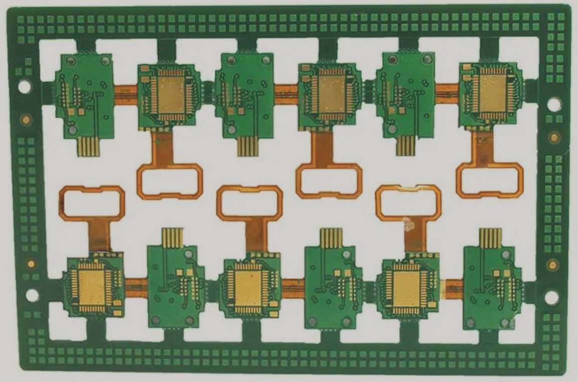
Understanding the Significance of PCB Gerber Files
When you order a Printed Circuit Board, timely delivery is crucial. The process of fabricating the board from your design file is intricate and time-consuming. Despite potential delays, the role of PCB manufacturers in translating and connecting your design concepts through Gerber files is indispensable for ensuring the quality and efficiency of the manufacturing process.
Decoding Gerber Files

The Gerber file format, developed by Gerber, has become the industry standard for PCB design software. It defines image conditions on the board, such as legend layers, soldermask layers, and conductor layers, essential for board fabrication.
Design professionals utilize CAS or EDA systems to create PCB layouts, detailing crucial manufacturing information. Without a Gerber file, manufacturers may lack comprehensive insights into your design, making the Gerber format vital for clarifying design requirements for every board image, applicable to PCB assembly and bare board creation.
For PCB assembly, incorporating a stencil layer into the Gerber format and controlling component locations are essential. The file serves as reference data for Surface Mount Technology (SMT) assembly, ensuring precision in the assembly process.
In essence, Gerber PCB files contain critical instructions for electrical engineering PCB design. Providing these files to your manufacturer post-design is crucial for accurate board production, emphasizing the importance of error-free documentation.
Gerber files come in three versions, with RS-274-D being the oldest, replaced by RS-274-X, and the latest format being Gerber X2, featuring attributes and stack-up data.
The Role of Gerber Files in PCB Design
Why PCB Design Engineers Need to Create Unique Gerber Files
PCB design engineers must create their own Gerber files for several reasons:
- When PCB manufacturers use different software applications, creating Gerber files becomes necessary to avoid delays.
- Even if both parties use the same software, creating unique Gerber files ensures reliability and timely delivery.
Generating Gerber Files: Essential for PCB Design Engineers
As a PCB design engineer, understanding how to generate Gerber files is crucial. Gerber data includes information for:
- Conductor layer
- Silkscreen layer
- Soldermask layer
Using Gerber Files for PCB Manufacturing
Technological advancements have revolutionized the PCB manufacturing sector. In the past, vector photoplotters were used to create tooling films, limiting design creativity. Now, modern laser plotters have replaced outdated systems, offering faster and more precise results.
Gerber files play a vital role in guiding the plotter during the manufacturing process. They provide instructions on plotter configuration and flash coordinates, ensuring accurate production of PCBs. Even with the shift to laser plotters, Gerber data remains essential for defining aperture details and configuration data.
Whether using old vector plotters or modern laser systems, Gerber files are indispensable for translating design specifications into tangible PCBs. By following Gerber instructions, plotter machines produce intricate details like pad dimensions, trace thickness, polygon fills, and lines accurately.
Advancements in Gerber Files for PCB Design
- PCB manufacturers are now utilizing laser imaging technology directly on copper for PCB image creation, eliminating the need for film.
- Database formats for PCB image design have become more familiar, providing detailed circuit board design data, including net connectivity.
- Despite new technologies, using Gerber files in their current format remains the safest option for PCB design.
Generating Gerber Files in PCB Design
After finalizing the design, the next step is to generate Gerber files for the contract manufacturer using PCB design software. While older software may require multiple steps for setup, modern CAD packages have streamlined the process.
Each layer of the board, including signal, solder mask, silkscreen, and solder paste layers, needs individual Gerber files. Manufacturers may add extra layers for the circuit board outline based on specific design requirements.
Before submission, ensure that standards, formats, and units are correctly set to align with manufacturing and design standards. Additionally, create an NC file to provide drilling instructions for the circuit board.
Documentation Post Gerber Files
When delivering files, document the Gerber PCB format and related manufacturing files to guide the manufacturer accurately. Assembly drawings and fabrications are essential for the manufacturing process. Collaborating with experienced engineers and designers can optimize the PCB design process and ensure high-quality results.


