Routing QFPs: Best Practices and Considerations
When designing PCB layouts, it’s crucial to pay attention to how you route QFPs (Quad Flat Packages) to ensure optimal performance and reliability. One common practice is to route tracks parallel to the pads rather than at 90-degree angles. This approach helps prevent potential soldering issues and ensures a cleaner connection between pins.
One practical reason for routing tracks parallel to the pads is to avoid solder bridges between adjacent pins. By extending the track outwards into the solder mask before connecting it to the neighboring pin, you can minimize the risk of short circuits and make troubleshooting easier.
According to industry standards, QFP tracks should exit parallel to the long edge of the pad or the pin’s direction when leaving the component body. This guideline helps maintain signal integrity and reduces the chances of signal interference.
However, when dealing with chips that have power pins on the corners, there may be opportunities to route traces at 90-degree angles to the pads. This layout configuration can streamline the routing process and allow for efficient placement of decoupling capacitors in the corners.
While traditional concerns like acid traps and under-etching have influenced routing practices in the past, modern etching processes have mitigated many of these issues. It’s essential to stay informed about the latest advancements in PCB fabrication techniques to make informed design decisions.
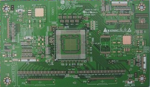
For a visual reference, check out the screenshot below illustrating different routing scenarios:


