Essential Guide to Selecting PCB Trace Width
Choosing the right trace width is crucial for PCB designers to ensure optimal performance and avoid potential issues. While software presets can work for simple circuits, complex designs require careful consideration. Incorrect trace width selection can lead to problems like overheating and circuit failure. Here are key factors to keep in mind:
- Current carrying capacity
- Space constraints
- Termination requirements
- Impedance control
Current Carrying Capacity
Understanding the maximum current a trace can handle is essential to prevent overheating and damage. Factors like copper thickness, trace location, and length play a role in determining the ideal trace width. Tools like the PCB Trace Width Calculator can simplify this process by providing guidance based on design parameters.
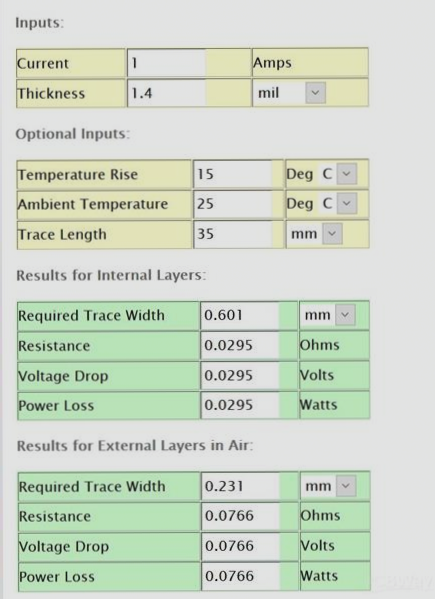
For multi-layer PCBs, inner layer traces may require wider widths due to limited heat dissipation capabilities. Thicker copper layers necessitate narrower traces for the same current capacity.
Space Constraints and Manufacturing
Minimizing PCB size helps reduce manufacturing costs, but designers must balance this with trace width requirements. Adhering to minimum trace width and spacing guidelines is crucial to avoid increased production costs. Signal traces typically range between 6 mils and 25 mils to ensure optimal performance.
Trace Termination
Proper termination of traces is essential to maintain signal integrity and prevent issues like reflections and signal degradation. Designers must consider factors like impedance matching and signal quality when terminating traces.
Trace Design Considerations for PCBs
When designing PCB traces, the width of a trace where it meets a pad is crucial. It is advisable to align the trace width with the pad size to maintain proper spacing between adjacent traces. This practice is commonly seen in SOIC component footprints, where trace widths are matched with pad widths to ensure clearances are maintained while routing.
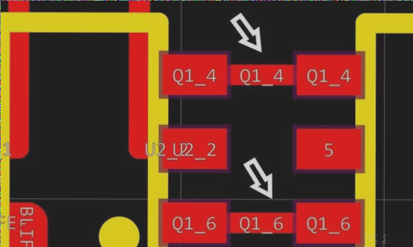
In the illustration, two traces are connected to a component pad with widths slightly narrower than the pad itself, allowing ample clearance between adjacent traces during routing. However, for more intricate components like BGAs (Ball Grid Arrays), selecting trace widths can pose a greater challenge.
Understanding Impedance Control in PCB Design
Impedance control is a critical consideration in high-frequency applications. At lower frequencies, trace impedance may not be a significant factor, and widths can be chosen based on current capacity or manufacturing constraints. Yet, with higher frequencies, PCB traces start behaving more like transmission lines due to the magnetic and electric fields they generate.
For high-frequency signals, it is essential to account for controlled impedance in trace design, which includes selecting the appropriate trace width. To delve deeper into this topic, exploring transmission line theory and PCB signal integrity is highly recommended for a comprehensive understanding.
I extend my gratitude to Wellcircuits for the opportunity to share this article.
For inquiries regarding PCBs or PCBA, please don’t hesitate to reach out to me at info@wellcircuits.com.