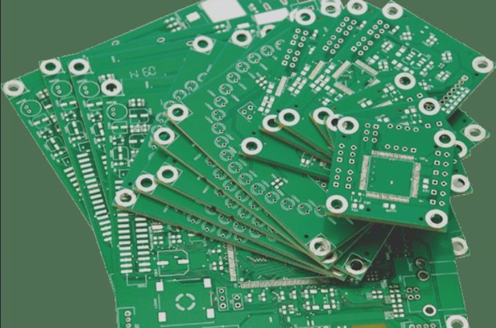
The Significance of High-Frequency Boards in PCB Production
High-frequency boards play a crucial role in circuit board production, especially in applications involving electromagnetic frequencies above 1 GHz. These specialized PCBs are designed to meet the increasing demands of modern technology, particularly in the microwave and millimeter wave frequency bands.
Applications and Importance
- Mobile communication products, power amplifiers, and low-noise amplifiers are some of the key applications for high-frequency boards.
- These boards are essential for passive components like power splitters, couplers, duplexers, and filters, as well as automotive anti-collision systems, satellite systems, and radio systems.
- The growing trend in electronic equipment development emphasizes the need for high-frequency boards to support higher frequencies.
Materials and Processing Methods
High-frequency board materials can be classified into two main categories:
Powder Ceramic-Filled Thermosetting Materials
- Manufacturers: Rogers 4350B/4003C, Arlon’s 25N/25FR, Taconic’s TLG series.
- These materials offer excellent electrical properties and chemical stability, crucial for high-frequency applications.
PTFE (Polytetrafluoroethylene) Material
- Manufacturers: Rogers’ RO3000 series, RT series, TMM series; Arlon’s AD/AR series, IsoClad series, CuClad series; Taconic’s RF series, TLX series, TLY series; Taixing Microwave’s F4B, F4BM, F4BK, TP-2.
- Processing methods for PTFE materials include cutting, drilling, hole treatment, PTH copper sinking, solder mask application, and gong board processing.
Processing Flow for PTFE Boards
The processing flow for PTFE boards involves a series of steps to ensure the quality and functionality of the final product:
NPTH PTFE Sheet Processing
- Cutting – Drilling – Dry Film – Inspection – Etching – Solder Mask – Characters – Spray Tin – Forming – Testing – Final Inspection – Packaging – Shipment.
PTH PTFE Plate Processing
- Cutting – Drilling – Hole Treatment – Copper Immersion – Board Electricity – Dry Film – Inspection – Diagram Electricity – Etching – Corrosion Inspection – Solder Mask – Character – Spray Tin – Molding – Test – Final Inspection – Packaging – Shipping.
Conclusion
High-frequency boards are essential components in modern electronic devices, enabling the operation of high-frequency and microwave systems. Understanding the materials and processing methods involved in manufacturing these boards is crucial for meeting the increasing demands of the technology industry.
Challenges in High-Frequency PCB Processing
- Immersion Copper:
- Line Gaps and Sand Holes:
- Green Oil Process:
- Board Surface Scratches:
One of the main challenges faced in high-frequency PCB processing is ensuring proper adhesion of copper to the walls of the holes.
High-frequency board processing involves difficulties in map transfer, etching, and controlling line widths due to line gaps and sand holes.
Issues arise in the green oil process related to adhesion and foaming, requiring special attention during PCB manufacturing.
Strict control measures are necessary at each stage of the process to prevent board surface scratches, which can impact the overall quality of the PCB.

