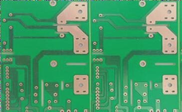
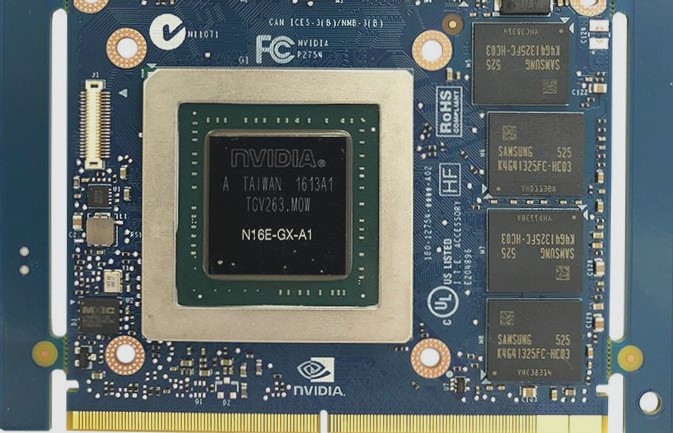
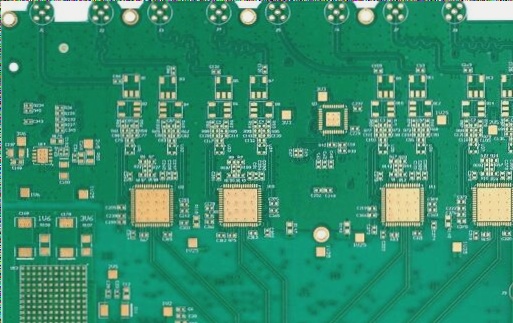
During the evolution and advancement of circuit board technology, reflow soldering has become a prominent trend. Interestingly, traditional through-hole components can also be integrated using reflow soldering, a process known as through-hole reflow soldering. This method offers the benefit of simultaneously completing all solder joints, thus reducing production costs. However, the use of reflow soldering is limited by temperature-sensitive components, whether they are interposers or SMDs. As a result, there has been a shift towards selective soldering in various applications post reflow soldering.
Characteristics of the selective soldering process can be best understood through a comparison with wave soldering. One significant difference lies in the fact that in wave soldering, the entire lower portion of the PCB is submerged in liquid solder, whereas in selective soldering, only specific areas come into contact with the solder wave. Due to the PCB’s poor heat conduction properties, neighboring components and PCB areas are not affected during soldering. Furthermore, flux must be applied prior to soldering. Unlike wave soldering, where flux is applied to the entire PCB, in selective soldering, flux is only distributed to the relevant areas. Moreover, selective soldering is suitable only for plug-in components, making it a novel and efficient method that requires a comprehensive understanding of the processes and equipment involved for successful implementation.
The selective soldering process typically involves flux spraying, PCB preheating, dip soldering, and drag soldering stages. The flux coating process is particularly crucial in selective soldering, as the flux must remain active to prevent bridging and PCB oxidation. Flux spraying is facilitated by an X/Y manipulator, which directs the flux nozzle to apply the flux onto the designated areas of the PCB. Various methods of flux application, such as single nozzle spray, micro-hole spray, and multi-point/pattern spray, can be employed. In the case of micro-point spraying, the diameter of the flux pattern should be greater than 2mm to ensure accurate deposition on the PCB with a position accuracy of ±0.5mm. It is vital to specify the amount of flux required, with a recommended safety tolerance range of 100% provided by the supplier.