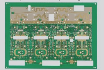
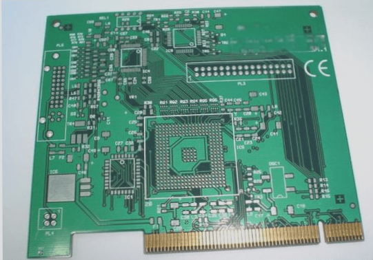
Key Steps for Successful PCB Routing
Before initiating the routing process, it is vital to conduct a comprehensive analysis of the design and configure the tool software correctly. This ensures that the final PCB design adheres to project specifications and fulfills performance expectations.
1. Determining PCB Layers
Deciding on the size and number of routing layers is a crucial initial step in the design process. The number of layers directly impacts trace routing and impedance. Opting for additional layers in modern PCB manufacturing allows for more efficient copper distribution and enhanced electrical performance.
2. Design Rules and Constraints
Successful PCB routing relies heavily on proper design rules and constraints to ensure all signal traces meet specified electrical parameters. Signal priority dictates routing rules, including trace width, via count, and signal interference constraints.
3. Component Layout
The component layout on the PCB should adhere to Manufacturability Design (DFM) principles for efficient assembly and optimal routing. Defining wiring constraints and signal layer configurations aids automatic routing tools in meeting engineering specifications.
- Power decoupling circuits should be placed near respective circuits to minimize interference.
- Power flow should be from the last to the first stage, with capacitors near the final stage.
- Current measurement points should be strategically located for easier debugging.
Regulated power supplies are best placed on separate PCBs to avoid noise interference.
4. Fan-Out Design
Ensuring each SMD pin is connected to at least one via during fan-out design supports inner connections, testing, and rework. Using larger vias and trace widths with optimal spacing enhances routing efficiency.
The routing path and testing requirements influence via selection for fan-out design.
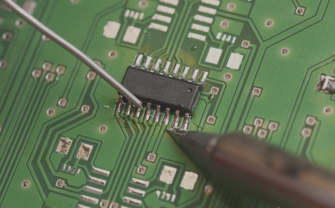
5. Manual Routing and Key Signal Processing
Manual routing complements automatic tools in PCB design. Critical signals should be manually routed or fixed before automatic routing to prevent interference. Grounding is crucial in high-frequency designs to avoid signal degradation.
High-Frequency PCB Layout Tips
When designing high-frequency circuits, it’s crucial to consider wire inductance and trace resistance. Wire inductance can lead to significant high-frequency voltage drops, especially with small currents. To address this issue, compact PCB layouts are essential, minimizing trace length to reduce noise.
Minimizing Interference
- Shortening signal trace length between layers.
- Organizing circuits by signal sequence to avoid signal path crossings.
- Ensuring perpendicular or crossed adjacent traces, not parallel, to reduce interference.
- Separating signal traces or using power and ground planes as shields to prevent parasitic coupling.
Automatic Routing Considerations
When using automatic routing tools, designers must consider electrical parameters like distributed inductance. Understanding these tools’ input parameters and effects ensures the routing quality meets expectations.
Setting Routing Constraints
General rules and constraints should guide signal routing. By specifying routing layers and via usage, the tool can automatically route according to the designer’s requirements. Once a design part is finished, it should be locked to prevent disruptions in subsequent routing stages.
Routing Complexity and Optimization
The circuit complexity and design rules determine the routing process. While automatic routing tools are efficient, manual intervention may be needed for certain signals. Optimization, such as shortening unnecessary long traces and reducing vias, can enhance performance and manufacturability.
If you have any inquiries about PCB or PCBA, don’t hesitate to reach out to me at info@wellcircuits.com.