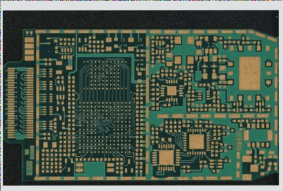
Signal Integrity in High-Speed Digital PCB Design
Signal integrity is a crucial consideration in the design of high-speed digital PCBs, with factors like component parameters, PCB characteristics, component placement, and signal trace routing impacting signal performance.
Key Aspects of Signal Integrity
- Signal integrity issues can lead to signal distortion, timing errors, incorrect data, and system malfunctions.
- Primary signal integrity issues include delay, reflection, synchronous switching noise, ground bounce, and crosstalk.
Definition of Signal Integrity
Signal integrity ensures signals maintain correct timing and voltage levels as they travel through a circuit, reflecting the quality of the signal along the path.
Delay
Delay is the time taken for a signal to travel along PCB traces, impacting clock pulse phase differences and signal edge arrival times.
Reflection
Reflection occurs when a signal’s delay time exceeds its transition time, leading to signal echoes on the transmission line due to impedance mismatches.
Synchronous Switching Noise (SSN)
SSN, or ground bounce noise, can occur when multiple digital signals switch simultaneously, affecting the power and ground planes due to IC characteristics and layout factors.
Crosstalk
Crosstalk refers to unwanted coupling between signal traces, causing interference and signal degradation in high-speed digital PCBs.
Crosstalk in PCB Design
Crosstalk, an unwanted coupling between signal lines, is a common issue in PCB design. It occurs due to mutual inductance and capacitance between lines, leading to noise interference. Capacitive coupling induces coupling current, while inductive coupling causes coupling voltage. Crosstalk noise can stem from electromagnetic coupling between signal traces, signal/power distribution systems, or vias.
Impact of Crosstalk
Crosstalk can result in problems like false clocks and intermittent data errors, degrading the transmission quality of adjacent signals. While complete elimination is challenging, controlling crosstalk within acceptable limits is crucial for system performance. Factors such as PCB layer parameters, trace spacing, driver/receiver characteristics, and termination methods all influence crosstalk levels.
Overshoot and Undershoot
Overshoot occurs when voltage exceeds the target value, either on rising or falling edges. Conversely, undershoot happens when voltage falls below the set value. Excessive overshoot can trigger protection diodes prematurely, while undershoot can lead to clock errors or data misoperation.
Ringing and Rounding
Ringing involves repeated overshoot and undershoot, caused by inductance and capacitance in the transmission line. It leads to oscillations in an underdamped state. On the other hand, rounding is an over-damped response. Both phenomena, influenced by reflections, can be mitigated with proper termination.
Ground Bounce Noise and Return Noise
Ground bounce noise arises from transient currents causing voltage fluctuations in the ground plane. It can interfere with other components’ operation. Factors like load capacitance, load resistance, ground inductance, and simultaneous switching devices impact ground bounce. Segmented ground and power planes in multi-voltage PCB designs require special attention to prevent return noise.