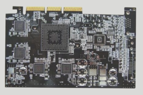
With the ever-faster edges of signals, the challenges faced by designers of high-speed digital PCB boards today were unimaginable just a few years ago. Signal edge changes of less than 1 nanosecond can lead to voltage variations between the power supply and ground layers on the PCB, impacting the power supply of the IC chip and causing logical errors. To ensure the proper functioning of high-speed devices, designers must mitigate these voltage fluctuations and maintain low-impedance power distribution paths. This can be achieved by incorporating decoupling capacitors on the circuit board to reduce noise from high-speed signals on the power and ground planes. Determining the number of capacitors needed, their values, and their placement on the board is crucial. Balancing the need for numerous capacitors with limited board space is a critical factor in the success or failure of the design.

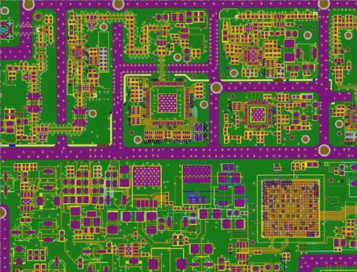
The trial-and-error design approach is time-consuming and expensive, often resulting in over-constrained designs that add unnecessary manufacturing costs. Utilizing software tools to simulate and optimize board designs and board resource usage is a more practical approach for designs that are iteratively tested for various board configurations. This article illustrates this process using the design of an xDSM (Dense Subcarrier Multiplexing) circuit board for a fiber/broadband wireless network. The software simulation tool utilizes Ansoft’s SIwave, based on a hybrid full-wave finite element technology, capable of importing board designs directly from layout tools Cadence Allegro, Mentor Graphics BoardStation, Synopsys Encore, and Zuken CR-5000 Board Designer. Figure 1 shows the PCB layout of the design in SIwave. As the structure of the PCB is planar, SIwave efficiently conducts a comprehensive analysis, providing outputs such as the board’s resonance, impedance, S-parameters of the selected network, and the equivalent Spice model of the circuit. The xDSM board’s dimensions, including the power and ground planes, are 11 x 7.2 inches (28 x 18.3 cm).
To understand the board’s design, consider its bare-board characteristics first, without any components mounted. Depending on the rise time of high-speed signals on the board, understanding the board’s behavior in the frequency domain up to 2GHz is essential. Figure 2 illustrates the voltage distribution when a sinusoidal signal excites the board to resonate at 0.54GHz, 0.81GHz, and 0.97GHz and above. Analyzing the voltage distribution between the power and ground planes in resonant mode at these frequencies provides a better understanding.
In resonant mode at 0.54GHz, the voltage difference between the power plane and the ground plane at the board’s center changes to zero. This behavior varies in different resonant modes, highlighting the importance of strategic device placement to avoid power integrity issues. For instance, by strategically placing devices requiring significant current changes at points with zero dropout characteristics, the resonance of the board can be managed effectively. Adding decoupling capacitors at appropriate locations helps maintain power integrity and reduce ground bounce noise over a wide frequency range.
Decoupling capacitors play a crucial role in managing voltage fluctuations caused by current spikes, ensuring that the power supply noise remains within acceptable levels. Frequency range considerations dictate the type and value of capacitors required. High-frequency ceramic capacitors cater to the MHz signal area, while larger electrolytic capacitors are suitable for kHz signals. Optimizing the PDS design through a combination of physical and virtual prototyping techniques enhances the overall power integrity of the circuit board.
Addition of ports at strategic locations and conducting broadband sweeps in SIwave allow for a detailed analysis of the board’s impedance characteristics. Simulation results aid in identifying areas where decoupling capacitors are needed to meet impedance requirements. Full-Wave Spice generates Spice-compatible circuit files for further analysis, incorporating models of components and capacitors to optimize power integrity. Analyzing the input and output ports, along with adding appropriate components, ensures that the circuit meets design specifications.
Simulation results display the power integrity curves of the IC chip, highlighting the effectiveness of strategic capacitor placement in reducing power supply noise. By analyzing each chip’s power integrity requirements, designers can ensure optimal circuit performance. By utilizing virtual prototyping methods and simulation tools, designers can streamline the design process, reduce costs, and optimize the power integrity design of PCB boards effectively.


