Important Parameters and Standards for PCB Boards
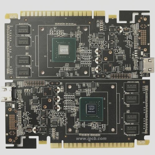
- PCB boards play a crucial role in the performance of electronic products.
- The implementation standard for six-type modules is EIA/TIA 568B.2-1.
- Key parameters include insertion loss, return loss, and near-end crosstalk.
Insertion Loss
Insertion loss is the signal attenuation along the transmission channel per unit length. It is influenced by signal frequency and transmission distance.
Return Loss
Return loss is caused by impedance changes in the product, leading to signal reflection. Higher return loss results in signal distortion and performance degradation.
Near-End Crosstalk (NEXT)
NEXT refers to signal coupling between transmission line pairs, affecting signal integrity. Capacitive or inductive coupling between adjacent pairs can lead to crosstalk.

Technology and Failure Mechanism
During the trial production of super six-type module PCB boards, theoretical guidance and computer-aided design are essential. Signal leakage from modules and plugs can lead to interference, which is addressed through balanced transmission and high-speed communication connector manufacturing technology.
The Importance of Addressing Signal Leakage in High-Speed Communication Connectors
- When it comes to connecting modules and plugs, balanced connection terminals are crucial to ensure efficient communication.
- Signal leakage and impedance losses in balanced lines can impede communication effectiveness.
- To combat external leakage, it is essential to study the E field and H field or utilize reverse attenuation methods in connector manufacturing.
E Field and H Field Interference
- Electromagnetic field interference on balanced lines is analyzed through E field and H field distributions.
- Testing parameters involve relative measurements under swept frequency for transmitting voice or data packets.
- Computer simulation technology plays a crucial role in analyzing and addressing this interference.
Strategies for Mitigating Signal Leakage
- To tackle socket signal leakage, signals within the concentration area need to be collected and returned based on simulation diagrams.
- Designing coupling capacitors and adjusting compensation line parameters are essential steps.
- Factors such as line length, distance, width, and layout must be considered for effective signal transmission.
Domestic Module Trial Production Processes
- Domestic manufacturers typically design compensation circuits post main circuit determination, followed by various scheme designs and sample productions.
- Enhancing performance through process improvements is crucial once the compensation circuit and PCB layer structure are finalized.
- Adjustments in interlayer gap parameters, copper foil thickness, and transmission line arrangement are key areas of focus.
- Implementing diagonal compensation methods for line pairs and optimizing process parameters at PCB processing plants are vital for successful module production.


