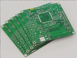
Common Mistakes in PCB Design and How to Avoid Them
- Utilize Inefficient Layout Techniques or Incorrect Components
- Neglect to Back up Your Work
- Operate as a Lone Island
With the advancement of technology, PCB design engineers now have the ability to create intricate designs by using smaller components and placing them closer together. Techniques like embedding discrete devices within internal PCB layers or using ball grid array (BGA) packaging with reduced pin pitch help in minimizing circuit board size and improving performance. Choosing the right circuit board layout technology during the design phase is crucial to prevent future issues and reduce manufacturing costs.
Backing up critical data is essential to prevent loss. Cloud-based data backup is a convenient and cost-effective solution to securely store important work results and files, reducing the risk of data loss due to theft, fire, or other disasters.
Collaboration is key in PCB design. While it may be tempting to work in isolation, seeking feedback from peers can help identify overlooked errors and provide valuable insights. Consulting with others ensures that unforeseen issues are addressed, the design stays on track, and costs are kept under control.
New Insights in PCB Design:
Recent developments in PCB fabrication have introduced innovative techniques such as embedding discrete devices within internal layers and using ball grid array (BGA) packaging with reduced pin pitch. These advancements have led to smaller circuit board sizes, improved performance, and efficient use of space. It is crucial to carefully select the right components and layout technologies to optimize design performance and minimize manufacturing costs.