Using 0.3mm Hole Vias in PCB Design: Is It Reliable?
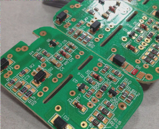
When designing a PCB, the choice of via hole size can significantly impact the layout and functionality of the board. While 0.5mm hole vias are commonly used, some designers are considering switching to 0.3mm hole vias to save space.
Although PCB manufacturers claim they can produce boards with 0.3mm holes, the real question is: Will using smaller vias cause connectivity issues?
Having previously used 0.3mm holes for non-critical connections like stitching and thermal purposes, the concern arises when a single via becomes crucial for a connection. Testing the connectivity of individual small vias within a network of many others can be challenging.
However, if past experiences with small vias have been error-free, there may be a possibility of scaling down the via size throughout the entire board. It ultimately boils down to the reliability and performance requirements of the specific PCB design.
Considerations for Using 0.3mm Hole Vias:
- Reliability of single via connections
- Testing methods for small vias
- Overall board performance with smaller vias
Conclusion:
While the idea of using 0.3mm hole vias for space optimization is tempting, thorough testing and consideration of the potential impact on connectivity are crucial before implementing this change in your PCB design.