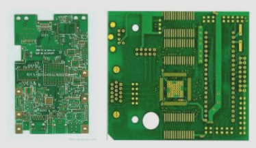
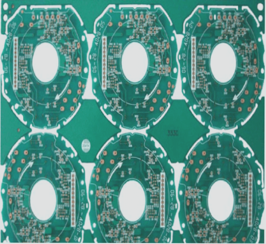
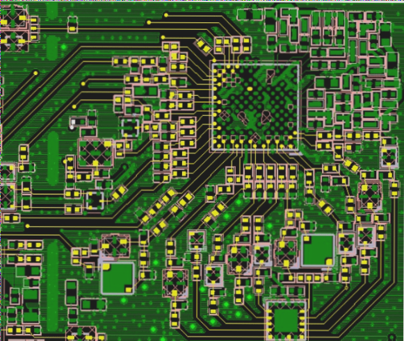
PCB design is a crucial aspect of any power supply’s development. The approach taken in its design directly influences the electromagnetic interference (EMI) and overall stability of the power supply. Thus, its significance is clear. This article will discuss PCB design techniques and specifications pertinent to LED drive power supplies.
(1) The workflow from schematic to PCB design involves: “establishing the principle netlist,” “setting design parameters,” “manual layout,” “manual routing,” “design verification,” “review,” and “CAM output.”
(2) Parameter setting requires that the spacing between adjacent traces meets electrical safety standards. To facilitate assembly and manufacturing, this spacing should be maximized. The minimum spacing must be adequate for the voltage levels involved. When wiring density is low, it is advisable to increase the spacing between signal lines. For signal lines experiencing significant voltage differentials,
—
If you need further adjustments or additions, just let me know!
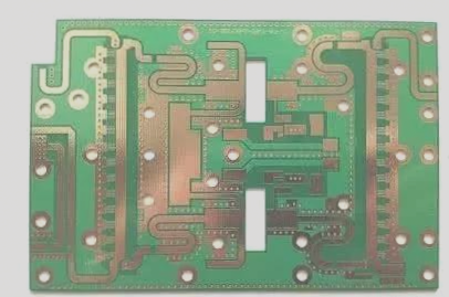
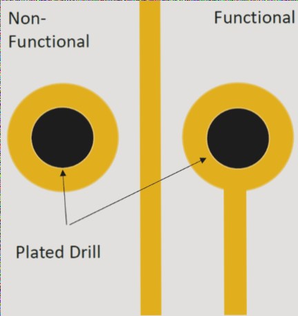
1. The spacing should be minimized, yet appropriately adjusted. Generally, set the trace spacing to 8 mil. The distance from the inner hole edge of the pad to the printed board’s edge should exceed 1 mm to prevent defects during processing. When connecting thin traces to pads, design the junctions in a drop shape. This design minimizes the risk of peeling and ensures reliable connections between pads and traces.
2. Component layout practices have demonstrated that even if the circuit schematic is accurate, improper PCB design can adversely affect the reliability of electronic equipment. For instance, if two thin parallel traces are positioned too closely, it may lead to signal waveform delays and reflection noise at the transmission line’s terminus; furthermore, inadequate power supply and ground considerations can degrade product performance. Thus, it’s essential to adopt correct methods when designing PCBs.
3. Wiring in switching power supplies includes high-frequency signals, meaning any printed line on the PCB can act as an antenna. The dimensions of these printed lines will influence their impedance and inductance, subsequently affecting frequency response. Even lines carrying DC signals may couple with radio frequency signals from adjacent traces, leading to circuit issues and potentially radiating interference.
4. After reviewing the wiring design, it’s crucial to verify whether it adheres to the designer’s established guidelines. Additionally, confirm that these guidelines align with the production process requirements for printed boards. Regularly check the distances between lines, pads, and through holes, ensuring they meet production standards. Evaluate whether the widths of power and ground lines are suitable and identify areas where the ground line can be widened on the PCB. Note that some errors may be overlooked, such as parts of connector outlines extending beyond the board frame, which can create spacing discrepancies. Moreover, each modification to wiring or vias requires copper to be reapplied.
5. The “PCB checklist” should include design rules, layer definitions, line widths, spacing, pad settings, and via configurations, while also emphasizing the rationality of device layout, power supply wiring, grounding networks, high-speed clock network routing and shielding, and the placement and connection of decoupling capacitors.

