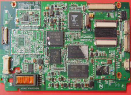
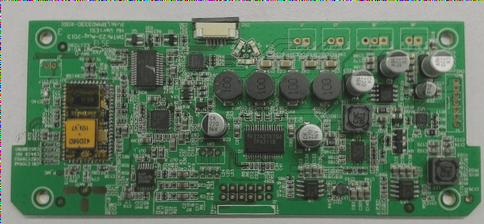
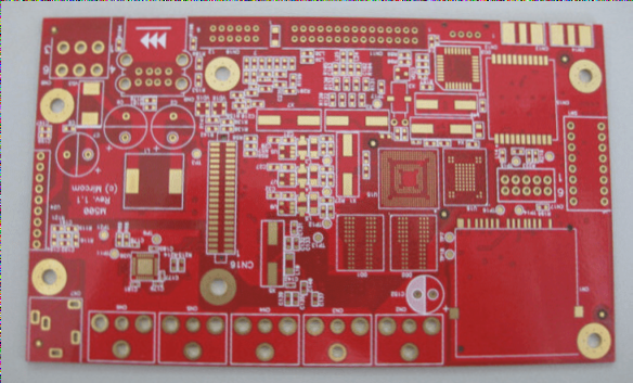
PCB Design Best Practices for Switching Power Supply
1. Parameter Setting
- Ensure proper spacing between traces for electrical safety and ease of production.
- Set trace spacing at 8 mils for optimal performance.
- Design thin trace connections with teardrop shapes to enhance peel resistance.
2. Component Layout
- Improper PCB design can impact electronic equipment reliability.
- Adhere to proper PCB design methods to avoid signal delays and interference.
- Place filter capacitors, power switches, and inductors close to minimize trace lengths.
3. Main Current Loops
- Each switching power supply has four current loops with specific functions.
- Precise placement of filter capacitors is crucial for energy management.
- Connect current loops directly to their respective filter capacitor terminals.
4. Layout Principles
- Consider PCB board size and shape for optimal performance.
- Avoid dense component placement to ease soldering.
- Arrange components evenly and compactly around functional circuit units.
- Position decoupling capacitors close to device VCC for high-frequency circuits.
- Arrange circuit units in line with signal flow for efficient signal circulation.
- Prioritize wiring efficiency and minimize wire routing for better performance.
Additional Information:
Recent studies have shown that incorporating advanced simulation software in PCB design can significantly improve the efficiency and reliability of switching power supplies. By simulating electromagnetic interference (EMI) and signal integrity during the design phase, engineers can identify and rectify potential issues before prototyping, saving time and resources.
Switching Power Supply PCB Design Best Practices
- High-frequency signals in switching power supplies make any PCB wire act as an antenna.
- Wire length and width affect impedance, inductance, and frequency response.
- Design AC-carrying traces to be short and wide to avoid interference.
- Trace length impacts inductance and impedance, adjust width accordingly.
- Grounding is crucial for stable operation and noise immunity.
Grounding Strategies:
- Single-point grounding: Connect filter capacitor common terminal to high-current AC ground points.
- Ground wire thickness: Use thick ground wires for stability amid varying currents.
- Input and output ground: Ensure mutual connection between input and output side grounds.
Inspection and Design Output:
- Verify adherence to design rules and production requirements.
- Rectify errors and follow PCB checklist standards.
- Generate Gerber files with required layers and settings.
Implementing these practices enhances reliability and performance consistency in switching power supply designs.