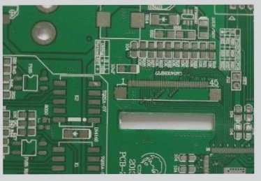
The Importance of Quality PCB Design for Effective SMT Processing
Effective SMT processing quality is closely tied to well-thought-out PCB design. By taking into account the characteristics and requirements of SMT production equipment and technology during PCB design, better SMT processing results can be achieved with less effort.
Key Requirements for SMT Processing Technology in PCB Design:
- The distribution of components on the PCB should be uniform to prevent localized low temperatures and soldering failures.
- Components on the PCB should be oriented in a consistent direction to streamline mounting, soldering, and testing processes.
- Adequate space should be allocated around larger components to accommodate SMD rework equipment.
- Heat-generating components should be positioned away from other components and supported to maintain distance from the PCB surface.
Additional Considerations for PCB Design and SMT Processing:
- Integrate heating components into multi-layer PCB designs using metal pads for heat dissipation.
- Maintain distance between temperature-sensitive components and heating elements to prevent damage.
- Arrange components requiring adjustments for easy access and avoid spatial conflicts.
- Position fixing holes strategically to accommodate thermal expansion and prevent warping.
- Increase spacing for components requiring secondary processing due to tolerances and precision.
- Ensure clearance for specific components to avoid contact with heating elements.
- Avoid placing stress-sensitive components in high-stress areas to prevent failures.
- Comply with soldering requirements to minimize shadow effects during soldering processes.
- Reserve space for positioning holes and fixing brackets on the PCB.
- Leave gaps in large-area PCB designs to prevent bending during soldering processes.
- Consider component orientation for reflow soldering based on the PCB’s entry direction into the oven.
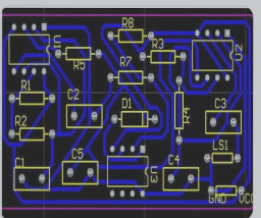
Best Practices for PCB Component Orientation
When it comes to designing a PCB, proper component orientation is crucial for ensuring efficient heating and performance. Here are some key guidelines to follow:
1. Orientation for Chip Components and SMD Pins
- For chip components and SMD pins, orient the long axis perpendicularly to the conveyor belt in the reflow oven.
- Ensure the long axis of SMD components runs parallel to the conveyor, with chip components perpendicular to each other.
2. Considerations for PCB Design
- For PCBs larger than 200mm:
- End chip components’ long axes should be perpendicular to the PCB’s long sides.
- SMD components’ long axis should align with the PCB’s long side.
- Components on both sides of double-sided assemblies should have identical orientations.
- Arrange similar components in the same direction for consistency in mounting, soldering, and testing.
3. Preventing Interlayer Shorts
- Maintain a minimum distance of 1.25mm between conductive patterns on the PCB’s inner and outer edges to prevent interlayer shorts.
- Avoid placing components and printed wires in structural areas if a ground wire occupies the PCB edge.
- Ensure no through holes are located in the bottom pad area of SMD/SMC to prevent solder remelting during wave soldering.
4. Component Installation Spacing
Component installation spacing should meet manufacturability, testability, and maintainability requirements for SMT assembly.
Following these guidelines will help optimize the performance and reliability of your PCB design. If you have any further questions, feel free to reach out!