1. SMT Patch Processing Overview:
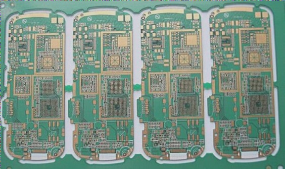
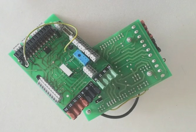
2. SMT patch refers to a series of technological processes applied to PCBs (Printed Circuit Boards). The Chinese name for PCB is “印刷电路板,” also known as a printed circuit board. It is a crucial electronic component that supports devices and provides electrical connections for electronic components. The term “printed” refers to the method of manufacturing the circuit board.
3. Mounter:
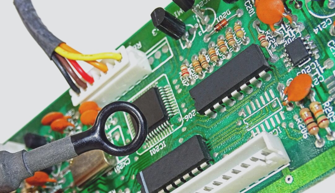
4. SMT, or Surface Mount Technology, is the most prevalent technology and process in the electronics assembly industry today. SMT involves surface mount components, which have no leads or very short leads (SMC/SMD in Chinese) that are mounted on the surface of a PCB or other substrates. This technology uses reflow soldering or dip soldering for assembly and soldering.
5. Typically, the electronic products we use are designed with PCBs and various capacitors, resistors, and other components according to a circuit diagram. Thus, various SMT chip processing techniques are required for production.
6. Basic SMT Process Components: Solder Paste Printing -> Component Placement -> Reflow Soldering -> AOI Optical Inspection -> Maintenance -> Sub-board.

1. Some people may ask why connecting an electronic component is so complex. This complexity is closely related to the development of our electronics industry.
2. Nowadays, electronic products pursue miniaturization, and previous perforated plug-ins cannot be reduced in size.
3. With the advancement of electronic products and integrated circuits (ICs), especially large-scale, highly integrated ICs, surface mount components are necessary.
4. Mass production and automation demand that factories produce high-quality products at low costs and high outputs to meet customer needs and enhance market competitiveness.
5. This involves the development of electronic components, integrated circuits (ICs), and the diversified use of semiconductor materials.
6. The revolution in electronic technology is imperative and must align with international trends.
7. For instance, Intel, AMD, and other international CPU and image processing device manufacturers have advanced production processes to over 20 nanometers, driving the development of SMT technologies.
8. SMT patch processing offers advantages such as high assembly density, smaller size, and lighter weight.
9. Patch components are about 1/10 the size and weight of traditional plug-in components, reducing product volume by 40%–60% and weight by 60%–80%.
10. SMT also provides high reliability, strong anti-vibration ability, low defect rate in solder joints, excellent high-frequency characteristics, reduced electromagnetic and radio frequency interference, and automation potential.
11. This processing method saves materials, energy, equipment, manpower, and time, and reduces costs by 30%–50%.
12. Due to the complexity of SMT patch processing, many specialized SMT patch processing factories have emerged.
13. In Shenzhen, the electronics industry’s growth has bolstered the prosperity of SMT patch processing.
14. **SMT Patch Processing Process:**
15. **Single-Sided Assembly:**
– Incoming inspection + silk screen + solder paste (red glue) + patch + reflow (curing) + cleaning + inspection + repair
16. **Single-Sided Mixed Installation:**
– Incoming inspection + PCB A side silk screen solder paste (red glue) + SMD + A side reflow (curing) + cleaning + plug-in + wave crest + cleaning + inspection + repair
17. **Double-Sided Assembly:**
– Incoming inspection + PCB’s A side silk screen solder paste (red glue) + patch + A side reflow (curing) + cleaning + flip board + B side silk screen solder paste (red glue) + patch + B side reflow (curing) or (DIP + wave crest) + cleaning + inspection + repair
18. **Double-Sided Mixed:**
– Incoming inspection + PCB’s B side silk screen solder paste (red glue) + patch + B side reflow (curing) + cleaning + flip board + A side silk screen solder paste (red glue) + patch + A side reflow (curing) or (DIP + wave crest) + cleaning + inspection + repair
19. **Basic SMT Process Components:**
– Screen printing (or dispensing), placement, reflow soldering, cleaning, inspection, and repair
20. **Silkscreen:**
– Prints solder paste or patch glue onto PCB pads, preparing for component soldering. The equipment used is a screen printing machine, located at the forefront of the SMT production line.
21. **Dispensing:**
– Drops glue onto fixed positions on the PCB to secure components. The equipment used is a dispenser, located at the forefront of the SMT production line or behind testing equipment.
22. **Mounting:**
– Installs surface mount components to fixed positions on the PCB. The equipment used is a placement machine, located behind the screen printing machine in the SMT production line.
23. **Curing:**
– Melts the patch glue to bond surface mount components to the PCB. The equipment used is a curing oven, located behind the placement machine in the SMT production line.
24. **Reflow Soldering:**
– Melts solder paste to bond surface mount components to the PCB. The equipment used is a reflow oven, located behind the placement machine in the SMT production line.
25. **Cleaning:**
– Removes solder residues, such as flux, from the assembled PCB board. The equipment used is a washing machine, which may be online or offline.
26. **Detection:**
– Inspects welding and assembly quality of the PCB board. Equipment includes magnifying glasses, microscopes, online testers (ICT), flying probe testers, automatic optical inspection (AOI), X-RAY inspection systems, and functional testers, located as needed on the production line.
27. **Rework:**
– Reworks PCB boards with detected faults. Tools include soldering irons and rework stations, configured at any production line position.
28. **Processed Component Specifications:**
– LGA, CSP, BGA, QFP, TQFP, QFN, PLCC, SOT, SOIC, 1206, 0805, 0603, 0402, 0201.
29. **Processing Modes:**
– PCB welding processing, lead-free SMT chip processing, plug-in processing, SMD chip, BGA soldering, BGA ball planting, BGA processing, chip packaging.
30. **Processing Includes:**
– Mobile phone boards, automobile testing equipment, B-ultrasound machines, set-top boxes, routers, network players, driving recorders, PLCs, display controllers, spectrum analyzers, and hairdressers.
31. **Main SMT Chip Processing Materials and Processes:**
– SMT processing of ordinary circuit boards (hard boards) and flexible circuit boards (soft boards). Technologies include solder paste process, red glue process, and red glue + solder paste dual process, with the dual process effectively addressing parts dropout issues seen with single red glue processes.
2. SMT patch refers to a series of technological processes applied to PCBs (Printed Circuit Boards). The Chinese name for PCB is “印刷电路板,” also known as a printed circuit board. It is a crucial electronic component that supports devices and provides electrical connections for electronic components. The term “printed” refers to the method of manufacturing the circuit board.
3. Mounter:
4. SMT, or Surface Mount Technology, is the most prevalent technology and process in the electronics assembly industry today. SMT involves surface mount components, which have no leads or very short leads (SMC/SMD in Chinese) that are mounted on the surface of a PCB or other substrates. This technology uses reflow soldering or dip soldering for assembly and soldering.
5. Typically, the electronic products we use are designed with PCBs and various capacitors, resistors, and other components according to a circuit diagram. Thus, various SMT chip processing techniques are required for production.
6. Basic SMT Process Components: Solder Paste Printing -> Component Placement -> Reflow Soldering -> AOI Optical Inspection -> Maintenance -> Sub-board.

1. Some people may ask why connecting an electronic component is so complex. This complexity is closely related to the development of our electronics industry.
2. Nowadays, electronic products pursue miniaturization, and previous perforated plug-ins cannot be reduced in size.
3. With the advancement of electronic products and integrated circuits (ICs), especially large-scale, highly integrated ICs, surface mount components are necessary.
4. Mass production and automation demand that factories produce high-quality products at low costs and high outputs to meet customer needs and enhance market competitiveness.
5. This involves the development of electronic components, integrated circuits (ICs), and the diversified use of semiconductor materials.
6. The revolution in electronic technology is imperative and must align with international trends.
7. For instance, Intel, AMD, and other international CPU and image processing device manufacturers have advanced production processes to over 20 nanometers, driving the development of SMT technologies.
8. SMT patch processing offers advantages such as high assembly density, smaller size, and lighter weight.
9. Patch components are about 1/10 the size and weight of traditional plug-in components, reducing product volume by 40%–60% and weight by 60%–80%.
10. SMT also provides high reliability, strong anti-vibration ability, low defect rate in solder joints, excellent high-frequency characteristics, reduced electromagnetic and radio frequency interference, and automation potential.
11. This processing method saves materials, energy, equipment, manpower, and time, and reduces costs by 30%–50%.
12. Due to the complexity of SMT patch processing, many specialized SMT patch processing factories have emerged.
13. In Shenzhen, the electronics industry’s growth has bolstered the prosperity of SMT patch processing.
14. **SMT Patch Processing Process:**
15. **Single-Sided Assembly:**
– Incoming inspection + silk screen + solder paste (red glue) + patch + reflow (curing) + cleaning + inspection + repair
16. **Single-Sided Mixed Installation:**
– Incoming inspection + PCB A side silk screen solder paste (red glue) + SMD + A side reflow (curing) + cleaning + plug-in + wave crest + cleaning + inspection + repair
17. **Double-Sided Assembly:**
– Incoming inspection + PCB’s A side silk screen solder paste (red glue) + patch + A side reflow (curing) + cleaning + flip board + B side silk screen solder paste (red glue) + patch + B side reflow (curing) or (DIP + wave crest) + cleaning + inspection + repair
18. **Double-Sided Mixed:**
– Incoming inspection + PCB’s B side silk screen solder paste (red glue) + patch + B side reflow (curing) + cleaning + flip board + A side silk screen solder paste (red glue) + patch + A side reflow (curing) or (DIP + wave crest) + cleaning + inspection + repair
19. **Basic SMT Process Components:**
– Screen printing (or dispensing), placement, reflow soldering, cleaning, inspection, and repair
20. **Silkscreen:**
– Prints solder paste or patch glue onto PCB pads, preparing for component soldering. The equipment used is a screen printing machine, located at the forefront of the SMT production line.
21. **Dispensing:**
– Drops glue onto fixed positions on the PCB to secure components. The equipment used is a dispenser, located at the forefront of the SMT production line or behind testing equipment.
22. **Mounting:**
– Installs surface mount components to fixed positions on the PCB. The equipment used is a placement machine, located behind the screen printing machine in the SMT production line.
23. **Curing:**
– Melts the patch glue to bond surface mount components to the PCB. The equipment used is a curing oven, located behind the placement machine in the SMT production line.
24. **Reflow Soldering:**
– Melts solder paste to bond surface mount components to the PCB. The equipment used is a reflow oven, located behind the placement machine in the SMT production line.
25. **Cleaning:**
– Removes solder residues, such as flux, from the assembled PCB board. The equipment used is a washing machine, which may be online or offline.
26. **Detection:**
– Inspects welding and assembly quality of the PCB board. Equipment includes magnifying glasses, microscopes, online testers (ICT), flying probe testers, automatic optical inspection (AOI), X-RAY inspection systems, and functional testers, located as needed on the production line.
27. **Rework:**
– Reworks PCB boards with detected faults. Tools include soldering irons and rework stations, configured at any production line position.
28. **Processed Component Specifications:**
– LGA, CSP, BGA, QFP, TQFP, QFN, PLCC, SOT, SOIC, 1206, 0805, 0603, 0402, 0201.
29. **Processing Modes:**
– PCB welding processing, lead-free SMT chip processing, plug-in processing, SMD chip, BGA soldering, BGA ball planting, BGA processing, chip packaging.
30. **Processing Includes:**
– Mobile phone boards, automobile testing equipment, B-ultrasound machines, set-top boxes, routers, network players, driving recorders, PLCs, display controllers, spectrum analyzers, and hairdressers.
31. **Main SMT Chip Processing Materials and Processes:**
– SMT processing of ordinary circuit boards (hard boards) and flexible circuit boards (soft boards). Technologies include solder paste process, red glue process, and red glue + solder paste dual process, with the dual process effectively addressing parts dropout issues seen with single red glue processes.


