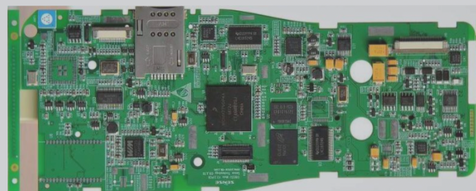
Motherboard Duplication Software: QUICKPCB 2005 V3.0
The QUICKPCB 2005 V3.0 software is a highly recommended tool for duplicating motherboards efficiently. It aligns with designers’ workflow preferences, enhancing design efficiency while minimizing testing challenges. The software boasts a high first-time success rate, ensuring reliable functionality.
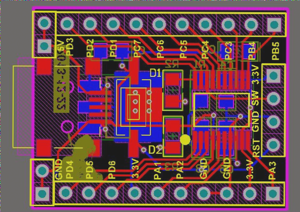
Key Features and Usage:
- Placement of pads, holes, traces, arcs, components, fills, POLYGONs, and text
- Attribute and grid settings for each element
- CTRL key for automatic snapping to the grid and element centers
- Shift key for selection, cut, copy, delete, rotate, mirror, and repeat operations
- Support for up to 32 layers with zoom display functionality
- Ability to set the origin at any location

Design Accuracy: 1 mil
The software supports the import of BMP and JPG images in its proprietary B2P format, automatically detecting BMP file resolutions. It also allows the management of component library files in Protel 2.5-2.8 format and supports the output of these files.
New Features in Software (Version 3.0):
- Added support for setting any blind or buried vias
- Ability to create a component library
- Functionality for custom components
- Support for vector-based characters
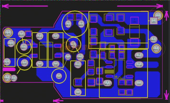
PCB Power and Ground Line Processing Technology
In PCB design, proper handling of power and ground lines is essential to minimize noise interference and ensure product quality.
Guidelines for Power and Ground Line Routing:
- Place a decoupling capacitor between power and ground
- Increase the width of power and ground lines, with the ground line ideally wider
- Use a wide ground line for digital circuits to create a grounding network
- Utilize a large copper area as a ground plane or allocate separate layers for power and ground in multi-layer PCBs
Inspection Guidelines
After completing the routing design, it is crucial to ensure that the design complies with established rules and production processes.
Verification Aspects Include:
- Proper spacing between traces, component pads, and vias
- Appropriate sizing and coupling of power and ground lines
- Optimal measures for critical signal traces
- Independent ground planes for analog and digital circuits
- Prevention of signal shorts from added graphics
- Adjustment of non-linear traces
- Adherence to PCB manufacturing standards
- Reduction of outer frame around power layers in multi-layer boards