Camera Module Testing for LGA Package Chip Solder Failure
A camera module is currently undergoing production testing to identify dysfunctional failures in the LGA package main chip. X-ray analysis will be conducted to further investigate the issue.

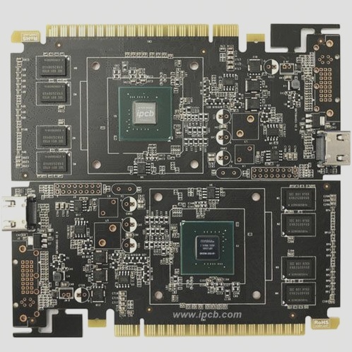
Understanding PCBs
PCB stands for printed circuit board and is a crucial component in electronic devices. The design and manufacturing of PCBs require specialized knowledge and technology, necessitating experienced experts for the task.
In the production process of PCBs, meticulous attention to detail and rigorous testing are essential to ensure quality.

Analysis Results
After testing, no significant abnormalities were found in the LGA welding of the two failed samples.
Staining Analysis
Sample 1 underwent LGA staining testing, revealing a small amount of tin phenomenon in most solder joints, indicating instances of poor virtual welding.

Cross-Sectional Analysis
Sample 2 showed poor soldering in multiple areas with minimal tin on the solder pads, suggesting false soldering.

SEM Analysis
SEM analysis revealed an IMC layer on the failed solder joints with minimal solder residue, indicating improper attachment to the device pads.

EDS Analysis
EDS analysis of the virtual solder joints did not show any abnormal elements.

Root Cause of Failure
Through various analyses, it was determined that the main cause of LGA soldering failure is the insufficient amount of solder paste reaching the bottom of the soldering joint.
Proposed Solutions
- Refine the printing stencil opening design and adjust printing process parameters for improvement.
- Verify the LGA chip mounting pressure.