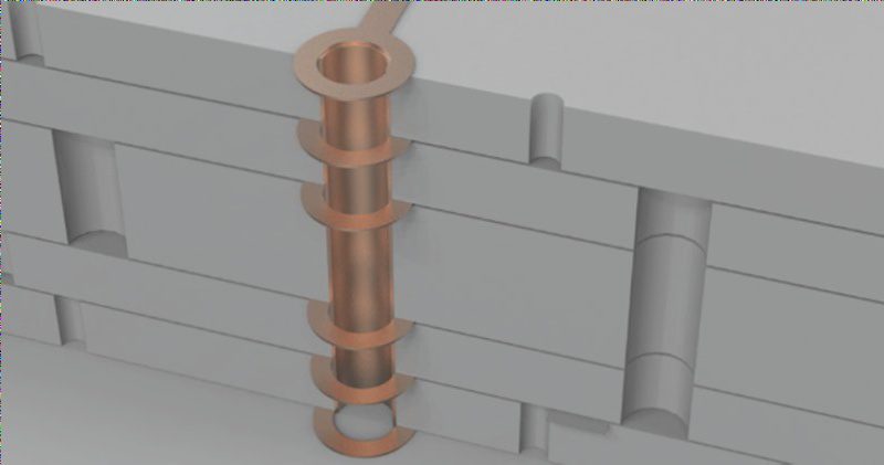
When delving into PCB design discussions, the topic of solder mask openings often surfaces. What exactly is solder mask opening in PCB design, when and how should it be employed? Below, we provide a comprehensive response to these inquiries.
1. What is Solder Mask Opening?In typical PCBs, the leads are coated with a protective layer to prevent short circuits and equipment damage. Solder mask opening involves removing this coating layer from specific wires, exposing them for tin application.2. Purpose of Solder Mask Opening in PCB Design:The utilization of solder mask openings in PCB design serves a dual purpose. Firstly, it transforms the PCB into a plug-and-play module. Additionally, it enhances solder thickness, catering to excessive current requirements. A common example is seen in memory chips, where golden fingers act as solder mask openings for easy plug-and-play functionality.3. Common Functions of Solder Mask Openings:Solder mask openings are not uncommon in PCBs, with memory chips being a prime example. Moreover, they are frequently employed in power boards and motor control boards to increase copper foil thickness for effective current handling.4. How to Implement Solder Mask Openings in PCB Design:In the realm of PCB design, the implementation of solder mask openings involves configuring threading and openings on the TOP/BOTTOM SOLDER layer. The TOP/BOTTOM SOLDER green oil layer is strategically placed to prevent tin contact with copper foil, ensuring insulation.
For solder pad openings, a default window is created during PCB design, exposing copper foil and expanding by 0.1016mm. This allows for seamless application of solder during the wave soldering process.Through-hole openings can also be designed with a window of 0.1016mm expansion for effective wave soldering. If preventing solder adherence to the solder mask is a concern, checking the PENTING option of the SOLDER MASK turns it off.Non-electrical wiring can be managed separately in this layer, allowing for the blocking of green oil and corresponding window openings. For copper foil lines, this enhances the wire’s ability to handle overcurrent by adding tin during the welding process. Non-copper foil lines, often reserved for logos and special characters, can be omitted to generate character screen layers.
In conclusion, solder mask openings are a crucial aspect of PCB design, serving both functional and practical purposes in ensuring optimal performance and adaptability. If you require services such as PCB fabrication or turnkey assembly, feel free to reach out for a quote and further assistance.


