The term “Solder Mask” is frequently encountered in articles and discussions about circuit boards. What exactly is Solder Mask? What role does it play in the circuit board?
What is Solder Mask?
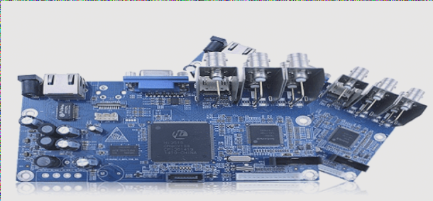
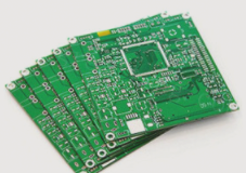
The proper Chinese name for Solder Mask is “solder mask” or “solder mask.” Since over 99% of circuit boards utilize green solder mask, it is often colloquially referred to as “green paint” or “green oil.” However, there are also red, black, and blue variants, among others. To accommodate different aesthetic needs, some R&D teams may use “red paint” during the NPI stage to differentiate from mass-produced boards. Exposed boards might opt for black to complement the color of their enclosures. With advancements in technology and the introduction of laser barcodes, it is generally advisable to stick with green solder masks, as they are more suitable for optical scanning. Interestingly, Solder Mask has a more vivid English term, “Solder Resist,” though it is less commonly used.
The Purpose and Function of Solder Mask
Solder Mask is applied to the top and bottom layers of the circuit board’s copper foil circuitry. Its primary function is to protect the copper foil from oxidation and accidental contact with solder, which could compromise the circuit board’s functionality. Typically, resin serves as the main material for Solder Mask, which is applied through PCB printing techniques to cover areas of the circuit board and the underside that do not require soldering. This ensures moisture resistance, insulation, solder resistance, high-temperature durability, and aesthetic appeal. In some cases, inkjet printing may be utilized.
—
Let me know if you need any further adjustments!

1. The term “Mask” in Solder Mask essentially denotes its function as a protective layer.
2. In the typical process of creating a Solder Mask, PCB manufacturers first apply the solder mask across the entire PCB, followed by a pre-baking phase. They then utilize a film for contact exposure, transferring the image onto the surface of the solder mask, akin to the operation of a photocopier.
3. It’s important to note that the image on the negative is inverted; the areas with black shadows are not meant to be preserved, while the transparent green paint remains intact. This process is why the term “mask” is employed in English.
4. Next, UV (ultraviolet) light is applied to cure the solder resist that is not covered by the mask. At this stage, the solder resist truly solidifies and adheres firmly to the circuit board. The previous drying step is merely “pre-drying.”
5. The board is then immersed in a chemical tank to wash away the masked areas. Consequently, the copper surfaces designated for soldering are exposed after this cleaning.
6. Please remember that only the copper surfaces become visible post the solder resist printing process. Subsequent surface treatments (such as gold, silver, or tin) are necessary to prevent oxidation of the exposed copper before soldering.
7. Solder Mask printing significantly influences the quality of SMT soldering.
8. Although the solder resist process appears straightforward, its primary purpose is to provide insulation and resist solder. However, improper application can lead to serious quality issues. Apart from the potential defects inherent in the PCB factory’s solder resist, such as poor cleaning, voids, incomplete prints, exposed copper, and uneven application, the offset and thickness of the solder mask can also critically affect SMT solder quality, particularly as components and solder joints on mobile phone boards become smaller.
9. ▪ Could the printed offset of the solder mask on the circuit board lead to BGA short circuits?
10. ▪ Do the thicknesses of the green paint and silk screen layers on the original PCB influence the amount of solder paste and contribute to BGA short circuits?
11. Since the Solder Mask employs film transfer to determine which areas retain the solder mask, the alignment between the Solder Mask and the PCB is crucial. If the alignment shifts excessively, the solder mask (ink) could obscure and alter the intended size of the exposed copper pads.
12. Furthermore, the height of the solder resist can affect the amount of solder paste applied. A thicker solder resist increases the height difference relative to the solder pad, which can lead to excessive solder paste application on smaller pads, heightening the risk of solder short circuits.
13. Process capabilities in Solder Mask printing are worth noting.
14. Most PCB manufacturers utilize scrapers and screens to apply the solder resist green paint on the circuit board. However, upon closer inspection, the circuit board’s surface is not as uniform as one might expect; it features copper foil traces and larger copper areas. These uneven surfaces can influence the thickness of the green paint application. Additionally, due to the nature of the squeegee, the corners of the circuit traces can sometimes be particularly thin.
15. PCB_Soldermask_thickness Most PCB manufacturers use scrapers and screens to apply the solder mask green paint. However, a careful examination reveals that the circuit board surface is not entirely flat, showing traces of copper foil and extensive copper areas. These variations can affect the thickness of the green paint applied, with the squeegee also contributing to potential thinning at corner locations (Trace corner, B).
16. Typically, PCB manufacturers implement basic size and tolerance controls for solder mask thickness at the four key positions outlined above, although the tolerance range can vary significantly between different manufacturers, with no established industrial standard. Generally, manufacturers avoid applying the solder mask green paint too thinly to prevent exposed copper and inadequate filling of via holes. Factors such as the type and pressure of the squeegee, along with the number of passes (usually one per round trip), can all impact the final thickness.
17. Additionally, while the thickness of the solder resist green paint is important, the accuracy of the printing position is even more critical. Due to current technology constraints, many PCB manufacturers rely on low-cost image copying techniques for solder resist green paint application. This often results in alignment inaccuracies, which can create challenges for systems requiring high precision. Unless prices are adjusted, higher-end imaging technologies remain out of reach.
18. The following outlines the capabilities of most PCB manufacturers regarding the offset in solder mask green paint printing and the minimum printable width of solder mask green paint:
19. The capabilities of most PCB manufacturers regarding solder mask green paint offset and minimum printable width are as follows:
20. ▪ E: Minimum solder mask dam/bridge: 4 mil (some manufacturers can achieve 3 mil). A solder dam refers to the solder resist green paint printed between two adjacent solder pads, primarily designed to prevent solder short circuits. Its name derives from its function; the height of the solder resist may not fully isolate solder overflow, but the surface tension of the solder resist is relatively lower compared to molten solder paste. Even if solder paste initially lands on the green paint, the solder’s strong cohesion typically causes it to retract into the solder pads, similar to how water flows downhill. Thus, printing solder resist green paint between adjacent pads can mitigate short circuit risks.
21. ▪ F: Tolerance for solder mask exposure registration: +/-2 mil (some manufacturers claim +/-1 mil). For “Non-Solder Mask Defined” wiring, this dimension accuracy is linked to the unilateral distance between the solder mask opening and the solder pad.
22. ▪ G: This dimension should correspond to E.
—
Let me know if you need any further modifications!


