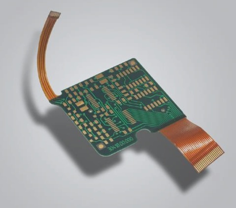
Seventy-five to eighty-five percent of the defects in SMT chip processing are caused by solder paste defects, making them a significant challenge in daily production. Proper control of details is essential, starting from initial BOM and Gerber data sorting, to component procurement channel management, and solder paste storage and access control, to solder paste printing, SPI solder paste inspection, reflow soldering, etc.
In order to prevent or minimize solder paste defects, it is crucial to strictly adhere to the requirements of quality management systems during SMT processing. For instance, in the patch processing of automotive electronics, implementing quality requirements for electrostatic control, component preservation, and solder paste storage and use can prevent electrostatic breakdown and ensure the quality of BGA and IC chips.
Due to the large batch sizes in PCBA processing, details such as the chip processing cycle, dry solder paste on the stencil, misalignment of the template opening and the circuit board, can lead to unwanted solder paste on the bottom of the stencil or result in poor soldering during the PCBA foundry process.
The following provides a brief introduction on how to avoid solder paste defects in SMT chip processing:
During the printing process on a fully automatic printing machine, ensure that the stencil is on the pad to guarantee a clean solder paste printing process. Damage to fine stencils due to bending of the stencil cross-section between thin pins can lead to printing defects and short circuits.
After printing solder paste in SMT packages, it is crucial to immediately address any printing errors as the solder paste becomes more difficult to remove the longer it dries. Improperly printed boards should be placed in an immersion solvent for easy removal of the solder paste before it dries.
To prevent solder paste and contaminants from remaining on the board’s surface, wiping with a clean cloth and scrubbing with a mild spray, followed by drying with a hot air blower is advisable. When using a horizontal stencil cleaner, ensure that the clean side is down so that the solder paste is removed from the board.


