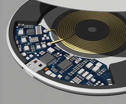
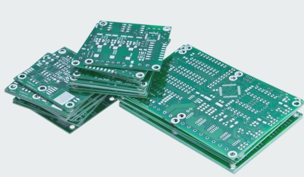
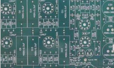
As a protective layer, the solder mask is applied to the traces and substrates that do not require soldering, preventing short circuits during the soldering process. Additionally, it provides a durable protective layer that is chemically resistant, ensuring a stable electrical environment. The quality of solder mask printing directly influences the overall appearance of the PCB.
Pre-treatment
Before applying the solder mask, the PCB must undergo pre-treatment. This step removes oxides, grease, and impurities from the surface, while also increasing the roughness of the board to improve ink adhesion, thus preparing the surface for printing.
Printing Solder Mask
There are two common methods for applying the solder mask: screen printing and electrostatic spraying. However, screen printing is the more widely used method. In this process, an automatic printing machine evenly spreads photosensitive ink onto the board’s surface through small holes in a screen, under the pressure of a squeegee. The tension and density of the screen, along with the angle, speed, and pressure of the squeegee, all affect the quality of the print.
Pre-drying
After each printing, the PCB is pre-dried to cure the solder mask ink. This step removes the solvent from the ink, preventing it from being tacky. The temperature and duration of pre-drying vary depending on the specific ink used.
Exposure
At this stage, both sides of the board are coated with solder mask ink. However, the ink is not needed on areas that must remain exposed for soldering, such as pads and plated-through holes. To remove the unwanted solder mask, an exposure and development process is performed. The solder mask film is aligned with the holes on the board, and the board is then placed in an exposure machine. The areas of solder mask exposed to UV light undergo a cross-linking reaction, hardening to form the solder mask layer, while the unexposed ink is washed away using an alkaline solution.
Developing
The unexposed ink is removed by the alkaline solution, leaving the desired solder mask pattern on the board. After completing the above steps, the board is baked in an oven at high temperatures (40-60 minutes) to fully cure the solder mask ink, ensuring it adheres strongly to the board surface and enhances its resistance to soldering.
If you have any questions about PCB or PCBA, please feel free to contact me at info@wellcircuits.com.


