There are numerous processes involved in the production of PCB circuit boards, and quality defects can arise at any stage. These quality issues often encompass various aspects, making them more challenging to address. The root causes of these problems are diverse, including chemical, mechanical, sheet metal, optical, and other factors. Drawing from decades of production experience and practical knowledge in addressing quality issues, along with relevant information on solving PCB technical problems, the following summary is provided:
**Defects, Causes, and Solutions in the Circuit Board Production Process**
| Process | Defects | Causes | Solutions |
|———|———|——–|———–|
| Film | Bubbles appear on the surface of the board. | The surface is not clean. | Check the board’s wettability; a clean surface should maintain an even water layer for up to 1 minute. |
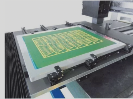
1. The temperature and pressure of the film are too low. Increase both temperature and pressure.
2. The edges of the film layer are raised. Excessive tension in the film layer leads to poor adhesion. Adjust the pressure screw.
3. The film has creases, indicating poor contact between the film and the board. Tighten the pressure screw.
4. Exposure is inadequate, resulting in poor resolution due to scattered and reflected light reaching the covered areas of the film. Reduce exposure time.
5. Overexposure occurs; decrease the exposure time.
6. There is a Yin-yang difference in the image; sensitivity is too low, leading to a minimum Yin-yang difference ratio of 3:1.
7. Poor contact exists between the film and the board surface. Inspect the vacuum system.
8. After adjusting, if light intensity remains insufficient, make further adjustments.
9. Overheating issues need to be addressed by checking the cooling system.
10. Switch from intermittent to continuous exposure.
11. The dry film storage conditions are inadequate; ensure working under yellow light.
12. Development reveals scum in the developing area due to insufficient development, leaving colorless film on the board. Slow down and extend the development time.
13. The developer’s concentration is too low; adjust to achieve 1.5-2% sodium carbonate content.
14. Excess film in the developer needs replacement.
15. The interval between development and cleaning is too long; it should not exceed 10 minutes.
16. Insufficient developer spray pressure requires cleaning the filter and checking the nozzle.
17. Overexposure necessitates correcting the exposure time.
18. Sensitivity issues arise when the maximum to minimum sensitivity ratio is below 3.
19. The film layer shows discoloration and lacks brightness due to insufficient exposure, which hinders polymerization. Increase exposure and drying time.
20. Overdevelopment requires a reduction in development time, correction of temperature and cooling systems, and checking developer content.
21. The film layer detaches from the board surface due to poor attachment from insufficient exposure or overdevelopment. Increase exposure time, decrease development time, and adjust the content.
22. The PCB surface is not clean; check surface wettability.
23. After exposure, proceed to development immediately; do not wait longer than 15-30 minutes.
24. Excess glue on the circuit pattern indicates the dry film may be expired; replace it.
25. Underexposure needs to be addressed by increasing exposure time.
26. The film surface lacks cleanliness; check the film quality.
27. Adjust the developer composition if it is inappropriate.
28. Development speed is too rapid; make necessary adjustments.
If you have any PCB manufacturing needs, please do not hesitate to contact me.Contact me

