Additive Process Addition
The additive process addition involves growing local conductor lines directly on a non-conductive substrate with a chemical copper layer, using an additional resistance agent. This method can be categorized into full addition, semi-addition, and partial addition.
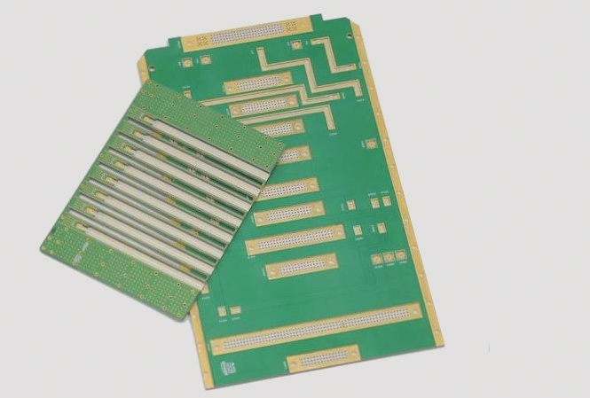
Backing Plates
Backing plates are thick circuit boards designed for plugging and making contact with other boards without soldering. The process includes inserting a multi-pin connector into press-fit through holes and wiring each guide pin of the connector. Since soldering is not possible on these specialized boards, the quality and aperture requirements are stringent, making it a niche industry in the United States.
Build-Up Process
The build-up process is a novel approach to thin multilayer plates that allows for the creation of multilayer boards without the costly mechanical drilling process. Various innovative technologies embracing layer-by-layer construction have gained traction in the U.S., Japan, and Europe, offering over ten products on the market. This method enables the production of thinner, denser, and more compact multilayer boards through sequential lamination.
Cermet Taojin
Cermet Taojin involves combining ceramic powder with metal powder and an adhesive to create a material that can serve as a resistor on the circuit board’s surface or inner layer, replacing external resistors during assembly.
Co-firing
Co-firing is the process of manufacturing ceramic hybrid circuit boards by printing circuits with various precious metal pastes on small boards and subjecting them to high-temperature firing, leaving behind interconnected lines of precious metal conductors.
Crossover Crossing
Crossover crossing refers to the vertical intersection of horizontal and vertical conductors on the board’s surface, filled with an insulating medium. This crossing can be created by adding a carbon film jumper or wiring above and below the layer.
- Create Wiring Board
- Dycostrate Plasma Etching Hole Increasing Layer Method
Advanced PCB Construction Techniques
Developed by Diconex, a company based in Zurich, Switzerland, the Dycostrate process involves etching copper foil at each hole position on the plate surface. The board is then exposed to a vacuum environment filled with CF4, N2, and O2, ionizing under high voltage to create a highly active plasma. This plasma etches the substrate at the hole positions to produce small pilot holes (below 10 mil).
Electro Deposited Photoresist
Electro Deposited (ED) photoresist is an innovative method that utilizes electroplating to evenly coat charged colloidal particles of optically sensitive resin onto the circuit board’s copper surface. This acts as an anti-etching inhibitor and is currently used in mass production for direct copper etching processes on inner plates. ED photoresist can function as either “anode type” or “cathode type” and is available in negative and positive working types. While negative working ED photoresist is commercialized for planar use, positive ED photoresist is under development in Japan for outer plates to facilitate the production of finer lines.
Flush Conductor Embedded Circuit
The Flush Conductor Embedded Circuit is a unique board with a completely flat surface and all conductor lines embedded within the plate. The circuit is created by etching part of the copper foil on a semi-cured substrate using an image transfer method. The surface circuit is then pressed into the semi-cured plate under high temperature and pressure, resulting in a circuit board with all flat lines embedded. This technology, also known as the etch and push method, produces a flush bonded board suitable for specialized applications like rotary switches and wiring contacts.
Frit Glass Frit
Glass powder is incorporated into thick film (PTF) printing paste along with precious metal chemicals to enhance agglomeration and adhesion during high-temperature firing. This process allows the printing paste on a blank ceramic substrate to form a solid precious metal circuit system.
Full Additive Process
The Full Additive Process involves growing selective circuits on a completely insulated plate surface through electrodeposition, mostly using chemical copper. This method is also known as the “full addition method” and should not be confused with “full electroless.”
- Hybrid Integrated Circuit
The Hybrid Integrated Circuit utilizes precious metal conductive ink applied to a small porcelain thin base plate through printing. After high-temperature firing to burn off organic materials, a conductor circuit is left behind. This technology serves as a circuit carrier between printed circuit boards and semiconductor integrated circuit devices, falling under thick film technology. Initially used in military or high-frequency applications, its growth has slowed due to rising costs and challenges in automatic production, alongside the increasing miniaturization and precision of circuit boards.
- Interposer Interconnect Conductor
An interposer supports two layers of conductors and can be connected by adding conductive fillers at the connection points. This includes filling bare holes of multi-layer boards with silver or copper paste or using materials like vertical unidirectional conductive adhesive layers.