PCB (Printed Circuit Board) and Its Importance in Electronics
PCB (Printed Circuit Board), also known as “印刷电路板” in Chinese, serves as a crucial platform for electronic devices, enabling them to function effectively. The production of PCBs involves electronic printing, hence the name “printed” circuit board.
Evolution from Point-to-Point Wiring to PCBs
In the past, circuits were constructed using point-to-point wiring, which had low reliability due to aging issues leading to breaks and short circuits. The introduction of PCBs revolutionized circuit design, offering durability and ease of maintenance through winding technology.
Advancements in Electronics Industry
With the transition from vacuum tubes to integrated circuits, electronic components became smaller and more affordable. This shift drove the widespread availability of electronic products in the consumer market, prompting manufacturers to adopt PCBs for compact and cost-effective solutions.
The PCB Production Process
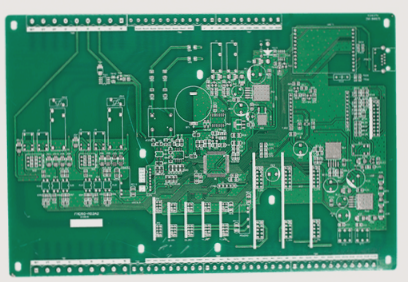
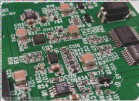
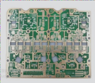
The PCB production involves a series of steps, including cutting, dry film application, exposure, etching, drilling, copper plating, solder mask application, and surface treatment. These processes culminate in the creation of functional PCBs.
Production Process of Double Panels
- Cutting: Trimming the copper clad laminate to prepare it for the production line.
- Paste Dry Film and Film: Applying a protective film on the board for subsequent processes.
- Exposure: Irradiating ultraviolet light onto the laminate with the film.
- Development: Using a developer to dissolve unexposed film areas.
- Etching: Removing unnecessary copper from the board.
- Removal of the Film: Washing off the dry film after etching.
- Drilling: Creating holes for pads and through-holes.
- Immersion Copper Plating: Plating copper onto pad holes and vias.
- Solder Mask Application: Applying a solder mask for protection and insulation.
PCB Production Process Overview
- Solder Mask: The application of green oil to non-soldered areas for insulation.
- Silk Screen Printing: Used for adding characters, logos, and text to the board.
The PCB production process is complex. For instance, in a four-layer printed board, steps include PCB layout, core board production, inner PCB layout transfer, core board punching and inspection, as well as pressing, drilling, copper chemical deposition on hole walls, outer PCB layout transfer, and outer PCB etching.