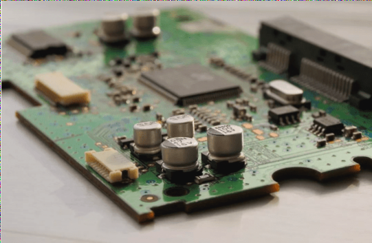
PCBA Appearance Quality Inspection Standards
PCBA appearance quality inspection standards detail the necessary materials, methods, and qualifications for producing high-quality solder joints and PCBA assemblies. These methods must consistently yield complete solder joints meeting specified criteria. This standard is essential for quality control and process personnel involved in PCBA manufacturing.
Latest Updates in PCBA Quality Inspection
Recent advancements in PCBA quality inspection include the integration of Artificial Intelligence (AI) for enhanced defect detection and improved inspection accuracy. AI algorithms can analyze solder joints with greater precision, leading to more reliable and efficient quality control processes.
Eligibility Judgment Criteria
- Optimal: Represents the highest quality level for PCBA appearance, emphasizing solder joint integrity, cleanliness, and overall aesthetics.
- Qualified: Indicates that the PCBA meets essential reliability and functionality standards, suitable for most production scenarios.
- Unqualified: Signifies that the PCBA fails to meet basic quality and reliability standards, requiring rework or rejection.
Process Change Qualification and Requirements
When implementing process changes, it is vital to ensure that the qualification requirements exceed the minimum standards necessary for the final product. This guarantees that any modifications maintain product integrity and functionality.
Enhanced Inspection Technologies
Implementing advanced inspection technologies, such as X-ray inspection systems and automated optical inspection (AOI) machines, can significantly improve the detection of defects in PCBA assemblies. These technologies enhance inspection accuracy and efficiency, ensuring high-quality standards are met consistently.
Important Considerations for Quality Control
Utilizing Automatic Inspection Technology (AIT) can streamline the inspection process by replacing manual visual inspections and complementing automated testing equipment. AIT enhances precision and consistency in quality control, leading to improved overall product quality.
Utilizing Standards for Quality Assurance
Integrating industry standards like IPC-A-610 and IPC-J-STD-001B into quality assurance processes can help manufacturers achieve higher levels of product quality and reliability. These standards provide guidelines for soldering, assembly, and inspection procedures, ensuring compliance with industry best practices.
J-STD-001B: Your Go-To Resource for Soldering Requirements
When quality or process engineers encounter disputes over inspection results on-site, consulting **J-STD-001B** can provide further clarity on soldering requirements.
Size and Dimensional Checks
- This standard does not include specific dimensional data for component installation or solder joint sizes. These aspects should be addressed separately, with exceptions handled through arbitration if needed.
- The focus is on ensuring that all processes and assembly steps align with established guidelines to maintain product functionality and quality.
PCBA Appearance Inspection Guidelines
Magnification Aids and Lighting:
- During PCBA inspection, optical magnification aids can be utilized to examine specific board details more closely.
- The chosen magnification should be accurate within ±15% of the selected level.
- Proper inspection lighting is crucial and should match the product’s size.
- For solder joint inspection, magnification selection is typically based on the minimum pad width of the device being examined.
- It is recommended to use higher magnifications for PCBA inspections with varying pad sizes to ensure no defects are overlooked.
PCB Orientation and Terminology
- Main Surface: This side houses the package and interconnection structures, often containing the most complex components. It is commonly known as the “component side” in through-hole insertion technology.
- Secondary Surface: This is the opposite side of the main surface, sometimes referred to as the “solder side” in through-hole insertion technology.
Electrical Spacing:
- To preserve design integrity, maintain wide spacing between conductors, conductive patterns, and materials.
- The standard specifies the “minimum electrical distance” to comply with corporate design codes and layout plans.
- Adequate component spacing helps prevent electrical interference and ensures long-term reliability.
If you have any inquiries regarding PCB or PCBA, feel free to contact me at info@wellcircuits.com.