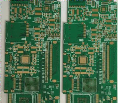
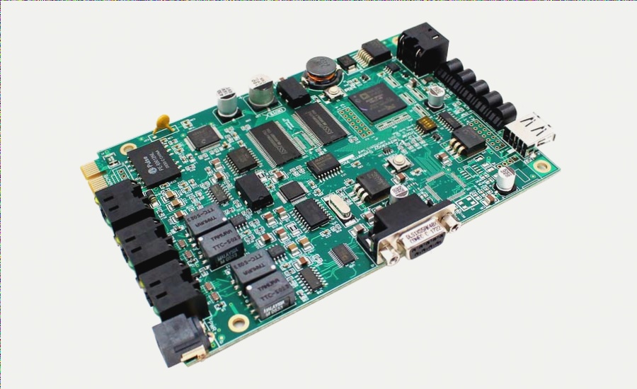
So, are you ready to design your first PCB prototype? This must be an exciting moment for you. We appreciate your eagerness to innovate and think outside the box. If you’re unsure about designing your PCB prototype on a low-cost PCB, this article is for you!
Here, we’ll provide you with a comprehensive understanding of PCB prototyping. Whether you’re a novice or an experienced engineer, these insights will be invaluable.
Let’s dive in.
Why the cost of a printed circuit board is a crucial factor
The cost of your printed circuit board (PCB) is a significant criterion. Higher costs translate to a more expensive final product. In fact, circuit boards can range in cost from 50 cents to $300 or more, depending on factors such as complexity, number of layers, and the installation requirements.
Aspect
To minimize the cost of your PCB prototype, controlling its size is essential. As the surface area of the PCB increases, so does its cost.
Similarly, designing an irregularly shaped PCB is generally more expensive than using traditional shapes. This is because the manufacturing process generates more waste with irregular designs.

Number of Layers
In fact, a higher number of layers in a PCB results in greater complexity, which in turn increases the overall cost of the process. Therefore, it is strongly recommended to minimize the number of layers as much as possible. A more effective approach is to stack additional PCB copper layers in a highway-like manner. This method provides a new plane for electronic routing and serves this purpose efficiently.
Material
To minimize the cost of PCB prototyping, it’s crucial to consider the type of material used. Standard PCBs are made of copper, with other commonly used materials including glass epoxy, known as FR-4. Here, “FR” stands for flame retardant, and the number indicates its flammability rating. FR-4 is the default choice for most PCB manufacturers. However, when dielectric constant and material thickness are critical for high-speed board parameters, careful consideration is required.
Electroplating Treatment
Through the pad electroplating process, the exposed copper surface of the PCB is coated with another metal material to enhance the solderability of the pad during assembly. Two standard technologies are HASL and ENIG. For low-cost PCB prototyping, sticking to HASL is advisable, as ENIG is significantly more expensive.
Board Thickness
The thickness of the PCB also significantly impacts the cost of manufacturing. The 1.6mm thickness is considered the industry standard, though it may increase depending on the number of copper layers. Thicker boards drive up production costs. While thick boards are expensive and offer limited functionality, thinner boards are more commonly used in mobile phones and other electronic devices. When designing a PCB, determine the required thickness early to avoid potential issues.
Impedance Control
If you plan to integrate technologies such as Bluetooth or Wi-Fi into the PCB, proper impedance control is essential. PCB impedance depends on factors like trace width, prepreg material, and solder mask. Proper impedance control is necessary to optimize wireless antenna performance. However, since most manufacturers do not offer controlled impedance by default, this may incur additional costs.
Hole Size
Determining the correct hole size on the PCB is crucial for establishing vertical electrical connections between copper layers. While smaller pads can save space and reduce costs, they can complicate the manufacturing process. Additionally, excessively small holes can result in tighter tolerances and increased waste, raising costs. It is best to maintain a balance and choose holes in the range of 0.2 – 0.3 mm.
Solder Mask
Applying a layer of polymer-like paint on the PCB’s copper traces prevents solder bridges and eliminates short circuit risks. A solder mask is essential. For cost-effective PCB design, you should choose the type and printing method of the solder mask carefully. Options include:
1. Epoxy liquid
2. Liquid photosensitive imaging
3. Dry film photosensitive imaging
4. Top and bottom masks
Select according to the specific requirements of your PCB design. For additional assistance, feel free to contact us—we are happy to help you choose the most suitable option.
Adhere to Industry Standard Sizes
To minimize costs, stick to industry standard sizes as much as possible. Most manufacturers follow these standards, and deviating from them may require custom adjustments, increasing the cost of PCB production. Adhering to standard sizes helps avoid unnecessary expenses.
Core Component Selection
For efficient prototyping, have a clear understanding of all the electronic components (e.g., sensors, microchips, displays, and connectors) you plan to use. The target price of the final product also plays a significant role. Create a detailed block diagram to ensure continuity and accuracy in your design. PCB design software can aid in preliminary design and documentation, allowing you to use PCBA calculators to estimate costs.
Circuit Design
Once you have a clear idea of your requirements and expectations, create a design schematic. Design applications can simplify this task and provide a better understanding of component connections. After drafting a preliminary schematic, contact us through the website for comprehensive information about your board.
Low-Cost PCB Bill of Materials
Once the PCB is manufactured, layout failures might occur, impacting the final product’s functionality. After completing several PCB layouts, generate a bill of materials, which can be automatically created by schematic design software. This document should include part numbers, quantities, and other specifications. Analyzing this bill can help identify the most expensive components for future analysis and improvement.
Low-Cost PCB Testing and Iteration
Retrieve the PCB from the manufacturer and thoroughly evaluate it. It is possible that the PCB may not meet your initial requirements, so be prepared for potential issues. Carefully weigh the choices and time needed for debugging. While this may be time-consuming, it is worthwhile for identifying and resolving problems related to PCB functionality.
In Conclusion
Designing a low-cost PCB prototype involves adhering to industry standards and following best practices to minimize costs. The choice of PCB manufacturer is also crucial—select one that accepts prototype orders, offers reasonable prices, provides discounts, and is equipped with the right tools to streamline manufacturing.
Here, we’ll provide you with a comprehensive understanding of PCB prototyping. Whether you’re a novice or an experienced engineer, these insights will be invaluable.
Let’s dive in.
Why the cost of a printed circuit board is a crucial factor
The cost of your printed circuit board (PCB) is a significant criterion. Higher costs translate to a more expensive final product. In fact, circuit boards can range in cost from 50 cents to $300 or more, depending on factors such as complexity, number of layers, and the installation requirements.
Aspect
To minimize the cost of your PCB prototype, controlling its size is essential. As the surface area of the PCB increases, so does its cost.
Similarly, designing an irregularly shaped PCB is generally more expensive than using traditional shapes. This is because the manufacturing process generates more waste with irregular designs.

Number of Layers
In fact, a higher number of layers in a PCB results in greater complexity, which in turn increases the overall cost of the process. Therefore, it is strongly recommended to minimize the number of layers as much as possible. A more effective approach is to stack additional PCB copper layers in a highway-like manner. This method provides a new plane for electronic routing and serves this purpose efficiently.
Material
To minimize the cost of PCB prototyping, it’s crucial to consider the type of material used. Standard PCBs are made of copper, with other commonly used materials including glass epoxy, known as FR-4. Here, “FR” stands for flame retardant, and the number indicates its flammability rating. FR-4 is the default choice for most PCB manufacturers. However, when dielectric constant and material thickness are critical for high-speed board parameters, careful consideration is required.
Electroplating Treatment
Through the pad electroplating process, the exposed copper surface of the PCB is coated with another metal material to enhance the solderability of the pad during assembly. Two standard technologies are HASL and ENIG. For low-cost PCB prototyping, sticking to HASL is advisable, as ENIG is significantly more expensive.
Board Thickness
The thickness of the PCB also significantly impacts the cost of manufacturing. The 1.6mm thickness is considered the industry standard, though it may increase depending on the number of copper layers. Thicker boards drive up production costs. While thick boards are expensive and offer limited functionality, thinner boards are more commonly used in mobile phones and other electronic devices. When designing a PCB, determine the required thickness early to avoid potential issues.
Impedance Control
If you plan to integrate technologies such as Bluetooth or Wi-Fi into the PCB, proper impedance control is essential. PCB impedance depends on factors like trace width, prepreg material, and solder mask. Proper impedance control is necessary to optimize wireless antenna performance. However, since most manufacturers do not offer controlled impedance by default, this may incur additional costs.
Hole Size
Determining the correct hole size on the PCB is crucial for establishing vertical electrical connections between copper layers. While smaller pads can save space and reduce costs, they can complicate the manufacturing process. Additionally, excessively small holes can result in tighter tolerances and increased waste, raising costs. It is best to maintain a balance and choose holes in the range of 0.2 – 0.3 mm.
Solder Mask
Applying a layer of polymer-like paint on the PCB’s copper traces prevents solder bridges and eliminates short circuit risks. A solder mask is essential. For cost-effective PCB design, you should choose the type and printing method of the solder mask carefully. Options include:
1. Epoxy liquid
2. Liquid photosensitive imaging
3. Dry film photosensitive imaging
4. Top and bottom masks
Select according to the specific requirements of your PCB design. For additional assistance, feel free to contact us—we are happy to help you choose the most suitable option.
Adhere to Industry Standard Sizes
To minimize costs, stick to industry standard sizes as much as possible. Most manufacturers follow these standards, and deviating from them may require custom adjustments, increasing the cost of PCB production. Adhering to standard sizes helps avoid unnecessary expenses.
Core Component Selection
For efficient prototyping, have a clear understanding of all the electronic components (e.g., sensors, microchips, displays, and connectors) you plan to use. The target price of the final product also plays a significant role. Create a detailed block diagram to ensure continuity and accuracy in your design. PCB design software can aid in preliminary design and documentation, allowing you to use PCBA calculators to estimate costs.
Circuit Design
Once you have a clear idea of your requirements and expectations, create a design schematic. Design applications can simplify this task and provide a better understanding of component connections. After drafting a preliminary schematic, contact us through the website for comprehensive information about your board.
Low-Cost PCB Bill of Materials
Once the PCB is manufactured, layout failures might occur, impacting the final product’s functionality. After completing several PCB layouts, generate a bill of materials, which can be automatically created by schematic design software. This document should include part numbers, quantities, and other specifications. Analyzing this bill can help identify the most expensive components for future analysis and improvement.
Low-Cost PCB Testing and Iteration
Retrieve the PCB from the manufacturer and thoroughly evaluate it. It is possible that the PCB may not meet your initial requirements, so be prepared for potential issues. Carefully weigh the choices and time needed for debugging. While this may be time-consuming, it is worthwhile for identifying and resolving problems related to PCB functionality.
In Conclusion
Designing a low-cost PCB prototype involves adhering to industry standards and following best practices to minimize costs. The choice of PCB manufacturer is also crucial—select one that accepts prototype orders, offers reasonable prices, provides discounts, and is equipped with the right tools to streamline manufacturing.


