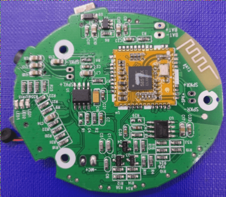
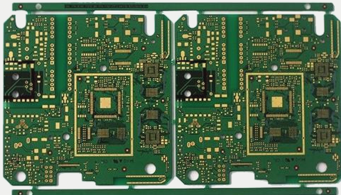
1. There are numerous processes involved in the manufacturing of PCB boards, and issues with quality may arise at various stages. These quality concerns can be complex and challenging to address. The root causes of these problems can stem from a variety of factors such as chemicals, machinery, sheet metal, optics, and more.
2. Drawing from decades of production experience and practical knowledge in resolving quality issues and technical challenges, the following outlines the defects, causes, and solutions in the PCB manufacturing process:

Film: If there are bubbles present in the film layer of the board and the board surface appears unclean, inspect the wettability of the board surface. A clean surface should maintain uniform water distribution, with a continuous water film lasting up to 1 minute.
If the film temperature and pressure are too low, elevate both temperature and pressure settings.
If the film edge lifts, it suggests poor adhesion caused by excessive tension. Adjust the pressure screw accordingly.
Film creasing may indicate inadequate contact between the film and the board surface. Tighten the pressure screw to improve contact.
For exposure issues such as poor resolution due to scattered and reflected light reaching the film cover, reduce exposure time. Conversely, in cases of overexposure, decrease exposure time.
Imbalance in image contrast (yin-yang difference) may result from low sensitivity, leading to a ratio of 3:1. Ensure sensitivity settings are appropriate.
When there’s poor contact between the film and the board surface, inspect the vacuum system.
If there’s insufficient light intensity after adjustments, readjust as necessary.
Check for overheating issues and inspect the cooling system.
For intermittent exposure issues, ensure exposure is continuous.
When dry film storage conditions are inadequate, such as exposure to yellow light, improve storage conditions.
In development, the presence of scum and insufficient development resulting in a colorless film remaining on the board indicate a need to slow down and increase development time.
Adjust the developer composition if it’s too low, aiming for 1.5-2% sodium carbonate content.
Replace the developer solution if there’s an excessive amount of film present.
Ensure the interval between development and cleaning does not exceed 10 minutes.
If there’s insufficient developer injection pressure, clean the filter and inspect the nozzle.
Correct exposure time if overexposure occurs.
Ensure proper sensitivity settings to maintain a sensitivity ratio of at least 3.
If the film appears discolored and lacks brightness due to insufficient exposure leading to inadequate polymerization, increase exposure and drying time.
In cases of excessive development, reduce development time, correct temperature settings, inspect the cooling system, and review developer content.
If the film is falling off the board, it suggests poor adhesion due to underexposure or overdevelopment. Adjust exposure and development times accordingly, and inspect leveling content.
Inspect the surface for dirt and ensure proper surface wettability.
After exposure, allow the film to sit for at least 15 to 30 minutes before development.
Replace dry film if excess glue is present on the circuit pattern, indicating expiration.
Increase exposure time if underexposure is observed.
Inspect the quality of the film if the surface appears unclean.
Adjust developer composition as needed.
If development speed is too fast, make adjustments on the PCB board to regulate the speed.
2. Drawing from decades of production experience and practical knowledge in resolving quality issues and technical challenges, the following outlines the defects, causes, and solutions in the PCB manufacturing process:

Film: If there are bubbles present in the film layer of the board and the board surface appears unclean, inspect the wettability of the board surface. A clean surface should maintain uniform water distribution, with a continuous water film lasting up to 1 minute.
If the film temperature and pressure are too low, elevate both temperature and pressure settings.
If the film edge lifts, it suggests poor adhesion caused by excessive tension. Adjust the pressure screw accordingly.
Film creasing may indicate inadequate contact between the film and the board surface. Tighten the pressure screw to improve contact.
For exposure issues such as poor resolution due to scattered and reflected light reaching the film cover, reduce exposure time. Conversely, in cases of overexposure, decrease exposure time.
Imbalance in image contrast (yin-yang difference) may result from low sensitivity, leading to a ratio of 3:1. Ensure sensitivity settings are appropriate.
When there’s poor contact between the film and the board surface, inspect the vacuum system.
If there’s insufficient light intensity after adjustments, readjust as necessary.
Check for overheating issues and inspect the cooling system.
For intermittent exposure issues, ensure exposure is continuous.
When dry film storage conditions are inadequate, such as exposure to yellow light, improve storage conditions.
In development, the presence of scum and insufficient development resulting in a colorless film remaining on the board indicate a need to slow down and increase development time.
Adjust the developer composition if it’s too low, aiming for 1.5-2% sodium carbonate content.
Replace the developer solution if there’s an excessive amount of film present.
Ensure the interval between development and cleaning does not exceed 10 minutes.
If there’s insufficient developer injection pressure, clean the filter and inspect the nozzle.
Correct exposure time if overexposure occurs.
Ensure proper sensitivity settings to maintain a sensitivity ratio of at least 3.
If the film appears discolored and lacks brightness due to insufficient exposure leading to inadequate polymerization, increase exposure and drying time.
In cases of excessive development, reduce development time, correct temperature settings, inspect the cooling system, and review developer content.
If the film is falling off the board, it suggests poor adhesion due to underexposure or overdevelopment. Adjust exposure and development times accordingly, and inspect leveling content.
Inspect the surface for dirt and ensure proper surface wettability.
After exposure, allow the film to sit for at least 15 to 30 minutes before development.
Replace dry film if excess glue is present on the circuit pattern, indicating expiration.
Increase exposure time if underexposure is observed.
Inspect the quality of the film if the surface appears unclean.
Adjust developer composition as needed.
If development speed is too fast, make adjustments on the PCB board to regulate the speed.


