**1.** PCB wiring plays a crucial role in the design of circuit boards within the manufacturing process. Achieving fast and efficient wiring while enhancing the aesthetic quality of your PCB layout is a topic worthy of exploration. This article outlines several key considerations for PCB wiring. Let’s identify any areas that may need improvement!
**2.** Common Ground Processing for Digital and Analog Circuits
In contemporary designs, many PCBs integrate both digital and analog circuits, rather than serving a single function. Thus, it is essential to account for potential interference between these two types of circuits during the wiring process, particularly concerning noise on the ground line.
**3.** Digital circuits operate at high frequencies, while analog circuits are highly sensitive. Therefore, high-frequency signal lines should be positioned as far away as possible from sensitive analog components. Regarding ground lines, the entire PCB should maintain a single point of connection to the outside environment. Consequently, the issue of a common ground for digital and analog signals must be addressed within the PCB itself. The digital and analog grounds on the board are effectively isolated from one another, connecting only at the interface (e.g., plugs) that links the PCB to the external environment.
**4.** A brief connection exists between the digital ground and the analog ground, but it is crucial to ensure that there is only one connection point. Additionally, non-common grounds may be present on the PCB, determined by the overall system design.
**5.** Signal lines should be routed on either the power layer or the ground layer.
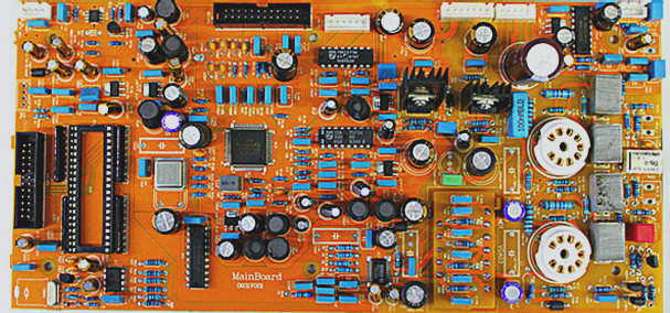
1. When designing a multi-layer PCB, if there are limited unallocated wires in the signal line layer, adding more layers may lead to waste, increased production workload, and higher costs. To address this issue, consider routing on the power or ground layers, prioritizing the power layer first to maintain formation integrity.
2. **Handling connection pads in large conductors**
In large ground or power areas, component pads need careful consideration. From an electrical standpoint, connecting component pads directly to the copper surface is preferable. Potential assembly risks include the need for high-power heaters during soldering, which can lead to cold solder joints.
3. To balance electrical performance and process requirements, utilize cross-patterned pads, often referred to as thermal pads, which significantly reduce the risk of cold solder joints from excessive heat during soldering. This processing is consistent for power connections and ground legs in multi-layer boards.
4. **The role of the network system in routing**
In many CAD systems, routing relies on the network system. A too-dense grid can increase path complexity and data volume, raising demands on storage and computing speed. Some paths may become invalid if obstructed by component pads or mounting holes.
5. Conversely, overly sparse grids can hinder distribution efficiency. A balanced grid system is essential, typically set at 0.1 inch (2.54mm) or its multiples (e.g., 0.05 inch, 0.025 inch, 0.02 inch) to facilitate efficient routing among standard component legs.
6. **Power and ground wire management**
Even with optimal PCB wiring, improper handling of power and ground wires can introduce interference, adversely affecting product performance and success rates. Therefore, careful routing of power and ground wires is critical to minimize noise and ensure product quality.
7. Engineers understand the noise generated between ground and power wires; a common solution involves adding decoupling capacitors between them. Maximize the width of power and ground wires, ideally making the ground wire wider than the power wire, with the hierarchy: ground wire > power wire > signal wire. Signal wire widths typically range from 0.2 to 0.3mm, with minimums of 0.05 to 0.07mm, while power wires range from 1.2 to 2.5mm.
8. For digital circuit PCBs, a wide ground wire can create a loop, forming a ground net. In contrast, analog circuits should avoid this method. Instead, utilize a large copper area as a ground wire, ensuring connections across the board. Alternatively, a multilayer board can designate one layer for power and another for ground wires.
9. **Design rule check**
Upon completing PCB wiring design, it is crucial to verify compliance with established rules while ensuring those rules align with production process requirements. Key inspection aspects include: the spacing between lines and component pads, lines and through holes, component pads and through holes, as well as the spacing between through holes. Additionally, assess whether the widths of power and ground wires are appropriate and if they are closely coupled.

