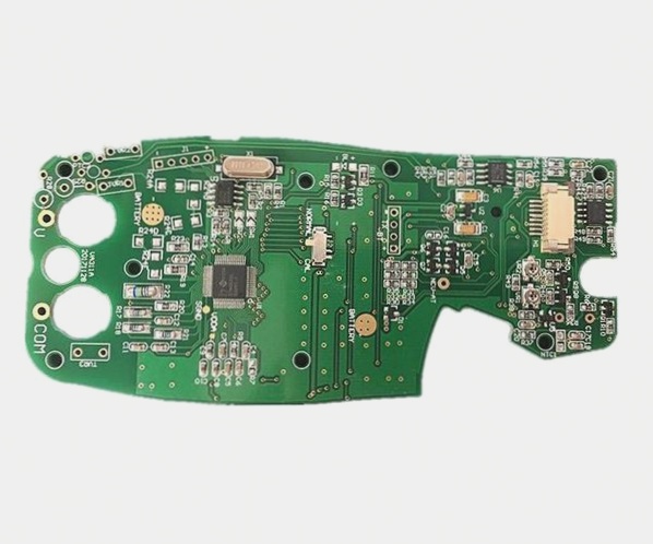
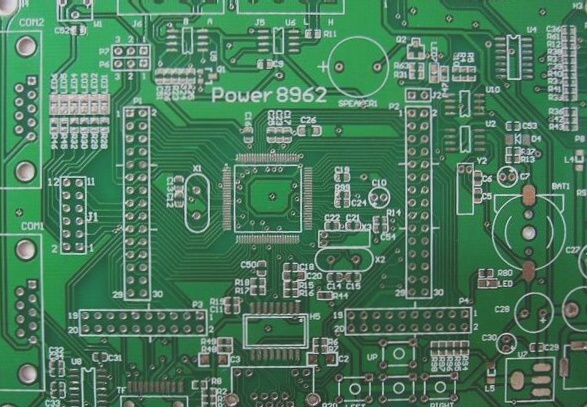
The Importance of Anti-Interference Design in PCBs
Anti-interference design plays a crucial role in ensuring the optimal performance of a printed circuit board (PCB). By implementing effective anti-interference techniques, engineers can enhance the reliability and stability of electronic devices. Here are some key strategies to mitigate interference:
1. Power Line Design
- Optimize the width of power lines to reduce loop resistance and enhance noise immunity.
- Align the orientation of power and ground lines with data transmission direction for improved performance.
2. Ground Wire Design Principles
- Segregate digital and analog grounds to minimize interference between circuits.
- Use thick ground traces to maintain stable ground potential and enhance noise immunity.
- Implement a closed-loop ground trace configuration for improved noise immunity in digital circuits.
3. Decoupling Capacitor Configuration
Decoupling capacitors are essential components in PCB layout design to manage power fluctuations and ensure signal integrity. Here are some best practices:
- Include a 10-100 µF electrolytic capacitor at the power input terminal to stabilize voltage.
- Add a 0.01 µF ceramic capacitor for each integrated circuit to suppress high-frequency noise.
- Utilize decoupling capacitors for components sensitive to power fluctuations, such as RAM and ROM memory devices.
- Keep capacitor leads short, especially for high-frequency bypass capacitors, to minimize inductance.
- Employ RC circuits for components generating spark discharges to protect sensitive electronics.
- Ground or connect unused CMOS input pins to maintain signal integrity and reduce noise interference.
By implementing these anti-interference techniques, PCB designers can enhance the performance and reliability of electronic devices, ensuring optimal functionality in various applications.