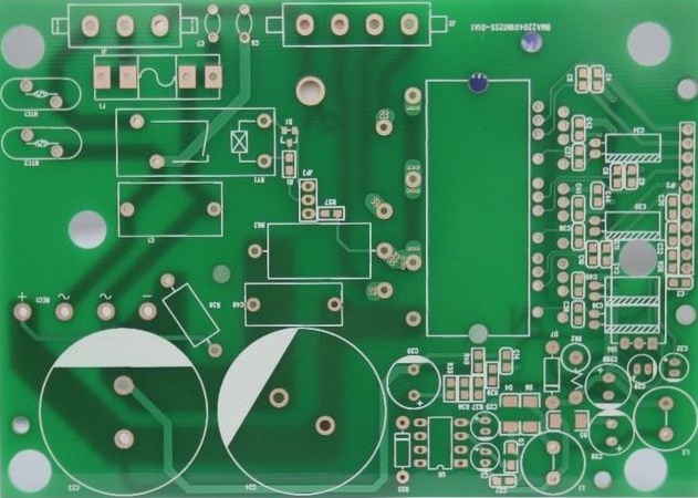
The interconnection of PCB board systems includes connecting chips to the circuit board, interconnections within the PCB board, and three types of connections between the PCB board and external devices. In RF design, the electromagnetic characteristics at the connection point are one of the main challenges faced by engineers. This article introduces various techniques for designing interconnections, including methods for mounting devices, isolating wiring, reducing lead inductance, and more.
There are signs indicating that the frequency of printed circuit board designs is increasing. As data rates rise, the bandwidth required for data transfer is pushing the upper limit of signal frequencies to 1 GHz and beyond. This high-frequency signaling technology extends beyond mmWave technology (30 GHz) to include RF and low-end microwave technology as well.
RF engineering methods must be capable of handling the stronger electromagnetic field effects that typically occur at higher frequencies. These electromagnetic fields can induce signals on adjacent signal lines or PCB board traces, causing unwanted crosstalk (interference and total noise), and impairing system performance. Return loss is primarily caused by impedance mismatches and can have the same effect on the signal as additive noise and interference. High return loss has two negative effects: 1. Signal reflections back to the source add noise to the system, making it more difficult for the receiver to distinguish the noise from the signal; 2. Any reflected signal essentially degrades the signal quality because the input signal shape has changed. Although digital systems are highly fault-tolerant since they only deal with binary data (1s and 0s), the harmonics generated when a high-speed pulse rises can weaken the signal at higher frequencies. While forward error correction techniques can mitigate some negative effects, part of the system bandwidth is used to transmit redundant data, resulting in reduced system performance. A more effective approach is to utilize RF effects to enhance rather than detract from signal integrity. Returns at recommended digital system frequencies (usually poorer data points). The total loss is -25dB, corresponding to a VSWR of 1.1.
The objective of PCB board design is to be smaller, faster, and more cost-effective. For RF PCB boards, high-speed signals may limit the miniaturization of PCB board designs. Currently, the primary methods for addressing crosstalk issues include ground plane management, spacing between traces, and reducing stud capacitance. The main approach to reducing return loss is through impedance matching, which involves effective management of insulating materials and isolation of active signal lines and ground lines, particularly where state transitions occur between signal lines and ground. Since the interconnection point is the weakest link in the circuit chain, addressing electromagnetic properties at the interconnection point is crucial in RF design. Each interconnection point should be thoroughly examined, and any existing issues should be resolved. The circuit board system interconnection involves three types of interconnections: chip-to-board, interconnections within the PCB board, and signal input/output between the PCB board and external devices.
Chip-to-PCB Interconnection:
High-speed chips, such as the Pentium IV, with numerous I/O interconnect points are already available. The chip’s performance is reliable, with processing rates reaching up to 1GHz. Methods for managing the increasing number and frequency of I/Os are well-known in the industry. The main challenge in chip-to-PCB interconnection is the high interconnection density, where the basic structure of the PCB material becomes a limiting factor for further growth. An innovative solution presented involves using a local wireless transmitter within the chip to transmit data to an adjacent circuit board. While the effectiveness of this solution is yet to be determined, it highlights that IC design techniques have advanced significantly beyond PCB board design techniques in high-frequency applications. Key skills and methods for high-frequency PCB board design include utilizing a 45° corner of the transmission line to reduce return loss, using high-performance insulating materials with controlled insulation constants, improving PCB design specifications for high-precision etching, avoiding tap inductance in protruding leads by using surface mount components, considering the layout of signal vias to prevent lead inductance, providing a rich ground plane connected with molded holes, utilizing electroless nickel or immersion gold plating processes, and incorporating solder mask for effective solder paste management.
For those unfamiliar with these methods, consulting with experienced design engineers, particularly those with experience in military microwave circuit boards, can provide valuable insights. Discussions with these engineers can also touch upon cost considerations and highlight more economical design options. While RF engineers may not typically focus on cost, their expertise can still be beneficial in finding cost-effective solutions. The training of new engineers who are inexperienced in dealing with RF effects will take time, and considering retrofitting computers to handle RF effects may also be a viable solution. Attention should also be given to addressing signal input/output issues between the PCB board and external devices. Companies like Trompeter Electronics, known for their innovative coaxial cable technology, are making strides in solving these problems by managing transitions between microstrip and coaxial cable designs. In both coaxial cables and microstrip configurations, ground plane management is crucial for effective signal transmission.