Optimizing PCB Interconnections for RF Design
When designing printed circuit boards (PCBs), it is crucial to optimize interconnections to mitigate RF effects. There are three main types of interconnections to consider: chip-to-board, intra-PCB, and PCB-to-external device connections.
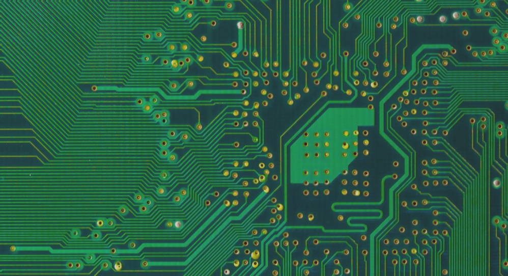
Chip-to-Board Interconnection
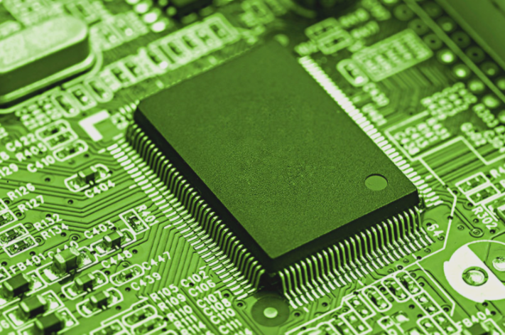
High-speed chips like Pentium IV with multiple I/O points pose challenges due to interconnection density limitations caused by PCB material constraints.
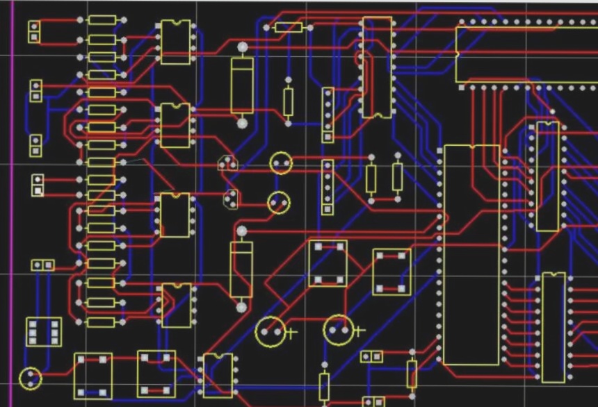
Intra-PCB Interconnection Techniques
- Using 45° transmission line corners to reduce return loss.
- Employing high-performance insulating boards with controlled dielectric constants for efficient electromagnetic field management.
- Specifying precise PCB design parameters for etching, including tight tolerances on line width, undercut, and cross-sectional shapes.
- Avoiding leaded components in high-frequency environments and opting for surface mount components.
- Avoiding plated through-hole (PTH) processing for signal vias to minimize lead inductance.
- Utilizing molded vias for connecting ground planes to manage 3D electromagnetic fields effectively.
RF Effects and Signal Integrity
With the trend towards higher frequencies in PCB designs, managing RF effects is crucial for signal integrity. Return loss, primarily caused by impedance mismatches, can lead to signal degradation and interference. Effective RF engineering methods are essential to handle intensified electromagnetic field effects at higher frequencies.
It is recommended to aim for a total return loss of -25dB in digital system frequencies to maintain signal quality. Strategies such as ground plane management, trace spacing optimization, and lead inductance reduction are essential to address crosstalk issues in RF PCBs.
Impedance matching plays a pivotal role in reducing return loss, requiring effective insulation material management and isolation of active signal lines from ground lines. Interconnection points are critical weak links in circuit chains, especially in RF design, where thorough examination and problem-solving are necessary to overcome electromagnetic challenges.
Enhancing Signal Integrity
While digital systems are fault-tolerant, harmonics generated during high-speed pulse rises can weaken higher frequency signals. Leveraging RF effects to enhance signal integrity rather than compromise it is a more effective approach than relying solely on forward error correction or redundant data transmission.
PCB-to-External Device Interconnection
Once onboard signal management challenges are resolved, the next step is to address the signal input/output transitions to external devices. This process involves transitioning from microstrip connections to coaxial cables. It is crucial to understand and manage impedance mismatches to reduce return losses, noise, and signal interference.
In essence, effectively managing impedance from PCB surfaces to connectors that terminate at coaxial cables becomes more complex as frequencies increase. Successfully addressing these challenges is essential for a well-designed PCB board, especially when transmitting signals across a wide range of frequencies.