If there are no vias, the PCB will not function. Vias are pathways that transmit signals between different PCB layers. During PCB manufacturing, a layer of copper is added to the substrate. This copper layer not only makes the traces conductive but also connects the layers through holes drilled into the board. The manufacturer can leave the via as is and use copper plating to transmit the signal, but to increase capacity, the via can be filled with another conductive material.
To create copper-filled vias, the manufacturer fills the vias with epoxy and copper. Although this process raises the cost of production, copper-filled vias make PCBs better suited for certain applications. These vias also offer advantages that other conductive fillers cannot. The following outlines the main uses of copper-filled vias and how they can enhance PCB design.
1. **Through Hole Filling Process**
When filling a via with copper, the manufacturer must ensure a uniform copper layer is formed without creating a layer that is too thick on the outside. If the process is not executed correctly, excess copper may accumulate, adding unnecessary weight or violating specifications, leading to defects or increased costs. As through holes become smaller, following these guidelines is crucial for meeting strict design standards.
The traditional method for copper via filling involves using pure copper. However, this often results in voids where contaminants can become trapped. When heated in later production stages, these voids can release gas, causing holes that disrupt the connection between copper layers. Modern methods to prevent this include leaving grooves in the filled vias or creating “X” patterns within them.
2. **Benefits of Copper-Filled Vias**
A PCB with copper-filled vias offers several advantages over one with only copper-plated vias:
– **Thermal Conductivity**: Copper-filled vias improve thermal conductivity. In high-temperature environments, managing heat away from the circuit board can prolong its lifespan and reduce defects. Copper’s high thermal conductivity helps draw heat away from sensitive areas of the PCB.
– **Electrical Conductivity**: Copper-filled vias are ideal for applications requiring the transfer of strong currents between layers. The conductivity of copper ensures that large currents can pass through deeper layers without overloading the PCB. This capability makes copper-filled vias essential in designs where higher voltages are necessary.
3. **Applications of Filled and Electroplated Vias**

Although PCBs with copper-filled vias offer greater capacity, they are more expensive to manufacture compared to PCBs with plated vias. In some cases, it’s also necessary to enhance the reliability of copper-filled vias. However, certain applications can still make use of copper-plated vias alongside copper traces.
When choosing the type of vias for your PCB, it’s important to consider the heat and voltage levels associated with the application. For low-stress applications, a qualified PCB with plated vias can perform perfectly well. On the other hand, PCBs with copper-filled vias are better suited for high-power, radio frequency, microwave, and LED applications, as these high-power integrated circuits require copper-filled vias to handle the current effectively.
**4. Copper, Silver Conductive Epoxy, and Gold-Filled Vias**
Beyond copper, PCB manufacturers can also opt for silver conductive epoxy to fill vias. However, while silver conductive epoxy may seem like a viable option, it is more expensive and not as efficient as copper. Alternatively, gold-plated vias can be used, but copper has several advantages over gold, including:
– Higher thermal conductivity
– Better electrical conductivity
– More cost-effective pricing
– Longer lifespan
– Greater reliability
– Superior performance in high-power applications
Even at a lower cost, copper-filled vias are generally a better choice than gold-plated vias. Their superior thermal and electrical conductivity allows them to dissipate excess heat more efficiently, while also handling higher voltages without the risk of overloading.
If you have any PCB manufacturing needs, please do not hesitate to contact me.Contact me
To create copper-filled vias, the manufacturer fills the vias with epoxy and copper. Although this process raises the cost of production, copper-filled vias make PCBs better suited for certain applications. These vias also offer advantages that other conductive fillers cannot. The following outlines the main uses of copper-filled vias and how they can enhance PCB design.
1. **Through Hole Filling Process**
When filling a via with copper, the manufacturer must ensure a uniform copper layer is formed without creating a layer that is too thick on the outside. If the process is not executed correctly, excess copper may accumulate, adding unnecessary weight or violating specifications, leading to defects or increased costs. As through holes become smaller, following these guidelines is crucial for meeting strict design standards.
The traditional method for copper via filling involves using pure copper. However, this often results in voids where contaminants can become trapped. When heated in later production stages, these voids can release gas, causing holes that disrupt the connection between copper layers. Modern methods to prevent this include leaving grooves in the filled vias or creating “X” patterns within them.
2. **Benefits of Copper-Filled Vias**
A PCB with copper-filled vias offers several advantages over one with only copper-plated vias:
– **Thermal Conductivity**: Copper-filled vias improve thermal conductivity. In high-temperature environments, managing heat away from the circuit board can prolong its lifespan and reduce defects. Copper’s high thermal conductivity helps draw heat away from sensitive areas of the PCB.
– **Electrical Conductivity**: Copper-filled vias are ideal for applications requiring the transfer of strong currents between layers. The conductivity of copper ensures that large currents can pass through deeper layers without overloading the PCB. This capability makes copper-filled vias essential in designs where higher voltages are necessary.
3. **Applications of Filled and Electroplated Vias**
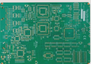
Although PCBs with copper-filled vias offer greater capacity, they are more expensive to manufacture compared to PCBs with plated vias. In some cases, it’s also necessary to enhance the reliability of copper-filled vias. However, certain applications can still make use of copper-plated vias alongside copper traces.
When choosing the type of vias for your PCB, it’s important to consider the heat and voltage levels associated with the application. For low-stress applications, a qualified PCB with plated vias can perform perfectly well. On the other hand, PCBs with copper-filled vias are better suited for high-power, radio frequency, microwave, and LED applications, as these high-power integrated circuits require copper-filled vias to handle the current effectively.
**4. Copper, Silver Conductive Epoxy, and Gold-Filled Vias**
Beyond copper, PCB manufacturers can also opt for silver conductive epoxy to fill vias. However, while silver conductive epoxy may seem like a viable option, it is more expensive and not as efficient as copper. Alternatively, gold-plated vias can be used, but copper has several advantages over gold, including:
– Higher thermal conductivity
– Better electrical conductivity
– More cost-effective pricing
– Longer lifespan
– Greater reliability
– Superior performance in high-power applications
Even at a lower cost, copper-filled vias are generally a better choice than gold-plated vias. Their superior thermal and electrical conductivity allows them to dissipate excess heat more efficiently, while also handling higher voltages without the risk of overloading.
If you have any PCB manufacturing needs, please do not hesitate to contact me.Contact me

