The Essential Steps in Circuit Board Manufacturing Process
For individuals new to circuit board design, understanding the production process is crucial for creating effective designs. Let’s delve into the key steps involved in circuit board manufacturing:
Step 1: Designing the Circuit Board Schematic
Begin by creating a schematic diagram that aligns with the circuit’s requirements and desired functions. It is essential to ensure that the components’ performance and functions are appropriately coordinated in the schematic design.
Step 2: Component Packaging with PROTEL Software
Once the PCB schematic is finalized, use PROTEL software to arrange the components uniformly, maintaining a consistent appearance and size.
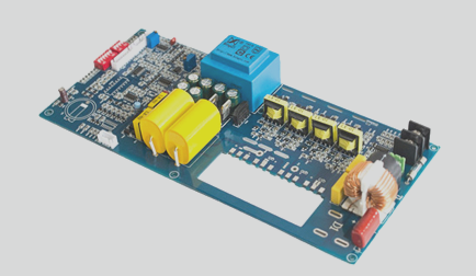
Step 3: Generating the Circuit Board Drawing
Position each component on the PCB panel according to dimensions, ensuring leads do not overlap. Conduct a DRC inspection to prevent crossover errors.
Step 4: Printing the PCB Diagram
Print the designed PCB diagram on carbon paper using an inkjet printer. Transfer the circuit diagram ink to a copper plate through a heat printing process.
Step 5: Manufacturing the Circuit Board
Etch away excess copper from the plate using a sulfuric acid and hydrogen peroxide solution. Punch holes and solder components onto the board.
Step 6: Testing and Troubleshooting
Conduct a thorough test on the circuit board, troubleshoot any issues, and make necessary repairs or replacements. Once testing is successful, the production process is complete!
If you require PCB manufacturing services, feel free to contact us. We are here to assist you in all your PCB needs.

