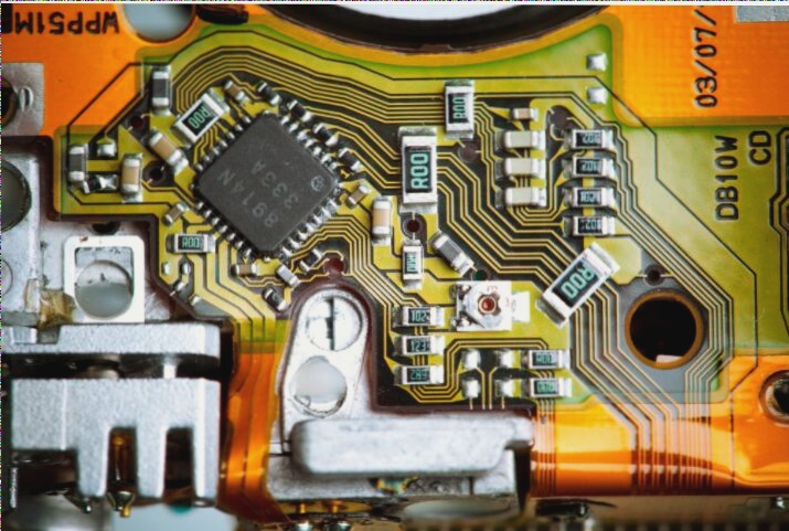
Proper termination of PCB traces is crucial to prevent signal reflection. If a trace is not adequately terminated (i.e., the impedance is not matched), the signal pulse from the driving end will be reflected back at the receiving end. This reflection distorts the signal waveform, leading to unexpected effects that can severely impact the system’s performance. In extreme cases, these distortions can cause errors, resulting in the failure of the PCB design. Moreover, reflected signals are more susceptible to external noise, further increasing the chances of system malfunction.
If these issues are not properly addressed during the design phase, Electromagnetic Interference (EMI) can become a significant problem. Increased EMI can degrade the performance of the PCB design itself and can also interfere with the operation of other systems. Therefore, attention to signal integrity through proper termination is essential not only to ensure design accuracy but also to maintain overall system reliability.
### Common Causes of Signal Reflection
The primary causes of signal reflection include:
1. **Long Trace Lengths**: Excessively long signal paths can lead to increased delay and higher chances of reflection.
2. **Improper Termination**: When transmission lines are not properly terminated or matched in impedance, reflections are more likely.
3. **Excessive Capacitance or Inductance**: High parasitic capacitance or inductance in the trace can also contribute to signal distortion and reflection.
4. **Impedance Mismatch**: A mismatch between the trace impedance and the connected components or transmission lines results in poor signal integrity.
### Signal Delay and Timing Errors
Signal delay and timing errors are another common issue in PCB designs, and they can severely impact the overall functionality. These errors manifest as delays in the signal transition between the high and low logic thresholds. When the signal does not change state promptly, it can lead to timing mismatches, causing functional errors in the devices.
Timing issues typically arise when multiple receivers are involved. The designer must calculate the worst-case time delays to ensure that the system operates within the expected timing constraints. Excessive delay may cause a failure to recognize the correct logic levels, leading to malfunction.
### Causes of Signal Delay
Several factors contribute to signal delay:
1. **Overloaded Drivers**: If the driver cannot source or sink enough current to quickly change the signal state, delays will occur.
2. **Excessive Trace Length**: Long traces increase the time it takes for signals to propagate, leading to delayed responses.
### Crossing the Logic Level Threshold Multiple Times
Another potential issue is the signal crossing the logic level threshold multiple times before stabilizing. This behavior can cause confusion in the logic interpretation by the receiver, leading to incorrect data being processed. This issue often occurs in high-speed designs where reflections or delays cause the signal to oscillate near the threshold voltage, resulting in multiple transitions.
### 5.3 Signal Reflection and Threshold Crossing Errors
Signal reflection errors occur when a signal crosses the logic level threshold multiple times during the transition process. This phenomenon is a specific form of signal oscillation that happens when the signal oscillates near the logic level threshold. When this occurs, the signal repeatedly crosses the threshold, leading to logic function disruption and errors in the system. Common causes of signal reflection include long trace lengths, unterminated transmission lines, excessive capacitance or inductance, and impedance mismatches. These issues can result in signal integrity problems, making it crucial to carefully manage trace length, impedance, and termination in PCB designs.
### 5.4 Overshoot and Undershoot
Overshoot and undershoot are typically caused by two factors: excessively long traces or fast signal transitions. While most components are equipped with input protection diodes to safeguard against these anomalies, there are cases where the overshoot can exceed the component’s power supply voltage range, potentially causing damage. Therefore, minimizing trace length and controlling the signal rise/fall times are essential in reducing overshoot and undershoot, ensuring both the longevity of the components and the stability of the signal.
### 5.5 Crosstalk
Crosstalk occurs when a signal in one PCB trace induces an unwanted signal in an adjacent trace. This can result in unintended interference, especially when signals are asynchronous or clock signals, which are particularly prone to crosstalk. To minimize crosstalk, it is important to manage trace spacing and ensure that traces are routed as far away from each other as possible, particularly from ground planes. Additionally, grounding techniques or shielding methods can be applied to prevent or reduce the interference. Carefully isolating sensitive signals and using proper PCB stack-up strategies can greatly reduce crosstalk effects.
### 5.6 Electromagnetic Interference (EMI)
Electromagnetic Interference (EMI) refers to the unwanted electromagnetic radiation emitted by a digital system, which can disrupt the operation of nearby electronic devices. EMI can be caused by high-frequency operating circuits or poor PCB layout design. The challenges of managing EMI are compounded by the difficulty and expense of using simulation tools, which are necessary to predict and control electromagnetic radiation. Although EMI simulation tools are available, they are often expensive and complex to configure, and the results may not always be practical. As a result, the best approach is to adhere to established design guidelines to control EMI, incorporating them throughout the design process. In high-speed PCB design, accumulated knowledge and experience play a significant role in controlling EMI, ensuring optimal performance without violating electromagnetic compliance standards.