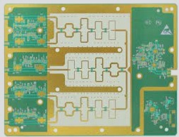
Radio Frequency (RF) Printed Circuit Board (PCB) Design: Balancing Guidelines and Practical Constraints
RF PCB design is often considered a complex task, with various guidelines to follow for optimal performance. The challenge lies in balancing theoretical principles with real-world constraints encountered during the design process.
Key Topics in RF Design
- Impedance and Impedance Matching
- Choice of Insulating Materials and Laminates
- Considerations of Wavelength and Standing Waves
These factors significantly impact the electromagnetic compatibility (EMC) and electromagnetic interference (EMI) of mobile phones.

Essential Requirements for RF Layout Design
- Isolate the high-power RF amplifier (HPA) and the low-noise amplifier (LNA) to minimize interference. Keep high-power and low-power RF circuits separate.
- Design partitions involve physical and electrical considerations:
- Physical partitions focus on component placement, orientation, and shielding.
- Electrical partitions include power distribution, RF traces, and grounding.
Physical Partitioning
Effective component placement along the RF path is crucial to minimize path length and separate high-power from low-power circuits. Utilizing a recommended board stacking approach and reducing unintended solder joints enhance RF performance.
RF and IF Traces
Minimize crossing between RF and IF traces with grounded spacing. Proper RF routing and component placement are vital for optimal PCB performance, especially in mobile phones.
Effective Decoupling
Proper decoupling of chip power supplies is essential for filtering out power supply noise and maintaining stable operation. Each chip may require multiple capacitors and isolation inductors for effective noise filtering.
Electrical Partitioning
Phones operating at multiple voltages require meticulous isolation to prevent cross-interference. Robust trace widths and proper decoupling ensure stable operation, particularly for high-power amplifier circuits.
Voltage Controlled Oscillators (VCOs) in PCB Design
Voltage Controlled Oscillators (VCOs) play a crucial role in converting voltage changes into frequency shifts, enabling rapid channel switching in electronic devices. However, they are sensitive to noise from control voltages. To address this issue, designers must focus on:
- Decoupling VCO power supplies effectively
- Minimizing interference with adjacent circuits
- Placing VCOs strategically towards the PCB’s RF edge
- Shielding VCOs when necessary
Power Supply and Ground Wiring in Mobile Phone PCBs
When designing PCBs for mobile phones, the layout of power supply and ground wiring significantly impacts product performance and reliability. Key considerations include:
- Incorporating decoupling capacitors between power and ground lines
- Widening ground traces more than power traces
- Utilizing large-area copper layers as ground planes
- Separating digital and analog grounds within the PCB
High-Frequency PCB Design Techniques
For high-frequency applications, specific design methods are essential to ensure optimal performance:
- Using 45° angle corners for transmission line paths
- Employing high-performance substrate materials
- Adhering to precise PCB design specifications for high-precision etching
- Preferencing surface mount components over leaded components
- Incorporating extensive ground planes with molded vias
Electromagnetic Compatibility (EMC) Design Strategies
Electromagnetic Compatibility (EMC) is critical for reducing interference and ensuring signal integrity. Designers should focus on:
- Optimizing wire width to minimize inductance
- Adopting correct wiring strategies to reduce inductance
- Suppressing crosstalk by strategic trace placement
- Mitigating electromagnetic radiation by proper grounding
- Implementing differential signal line routing
By following these guidelines, designers can improve the performance, reliability, and electromagnetic compatibility of mobile phone PCB designs.