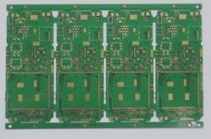
Radio frequency (RF) printed circuit board (PCB) design is often referred to as a “black art” due to its theoretical uncertainties. However, this perception is only partially true. There exist numerous guidelines for RF circuit board design that should not be overlooked. Yet, the true challenge lies in navigating these guidelines and principles when they cannot be precisely adhered to due to various design constraints.
There are several critical topics in RF design that merit discussion, such as impedance and impedance matching, materials for insulating layers and laminates, as well as wavelength and standing waves. These factors significantly influence the electromagnetic compatibility (EMC) and electromagnetic interference (EMI) of mobile phones. The essential conditions to consider when designing an RF layout are summarized as follows:
—
This revision aims to clarify and streamline the original text while maintaining its technical focus on RF PCB design.

1. The high power RF amplifier (HPA) and the low noise amplifier (LNA) should be separated. To maximize isolation between the high power RF amplifier (HPA) and the low noise amplifier (LNA), it’s crucial to physically distance the high power RF transmit circuit from the low power RF receive circuit. Mobile phones are packed with functions and components, demanding highly skilled design due to PCB space constraints and wiring limitations. In such cases, opting for a four-layer to six-layer PCB and staggering their operations rather than simultaneous use may be necessary. High power circuits, which may also include RF buffers and voltage controlled oscillators (VCOs), require dedicated ground planes on the PCB without any vias to ensure integrity, preferably with ample copper coverage. Analog signals should be kept well apart from high-speed digital and RF signals to prevent interference.
2. Physical and electrical partitioning is essential for effective design. Physical partitioning involves strategic component placement, orientation, and shielding, while electrical partitioning focuses on power distribution, RF traces, sensitive circuits, and grounding.
2.1 In physical partitioning, optimizing component placement is critical in RF design. Placing components along the RF path and adjusting their orientation minimizes path length, separates input from output, and isolates high power from low power circuits. A preferred board stacking method involves placing the main ground plane on the second layer beneath the surface layer and routing RF lines on the surface layer to reduce path inductance and minimize unintended solder joints on the main ground. Linear circuits like multistage amplifiers can effectively isolate RF zones, but duplexers, mixers, and IF amplifiers/mixers require careful planning to minimize interference.
2.2 RF and IF traces should cross minimally, with ample ground spacing between them. Component placement in mobile phone PCBs often situates the low noise amplifier on one side and the high power amplifier on the opposite side, connected via a duplexer to the antenna. Proper vias and shielding techniques are crucial to prevent RF energy transfer across the board. Metal shields, when used, should be grounded and positioned to maximize effectiveness without compromising PCB space.
2.3 Effective chip power decoupling is crucial for RF chips sensitive to power supply noise. Integrated circuits may necessitate multiple capacitors and inductors per chip to filter out power supply noise effectively. Decoupling capacitors and inductors should be strategically placed to minimize mutual inductance and interference, ensuring stable circuit performance across varying conditions.
2.4 Electrical partitioning principles, akin to physical partitioning, emphasize segregation of high and low voltage parts controlled by software for power efficiency. Power enters via connectors, undergoes immediate decoupling to filter external noise, and then distributes through switches or regulators. While trace width is usually sufficient for mobile phone PCBs, a separate wide trace is essential for high-power amplifier supply to mitigate voltage drop. Proper grounding and decoupling at high power amplifier pins prevent noise radiation and ensure stability.
2.5 Voltage Controlled Oscillators (VCOs) and resonant circuits require meticulous design to minimize noise. VCOs, often shielded and placed at the RF board’s end, convert control voltage to frequency changes, influencing RF signal noise levels. Resonant circuits, crucial for setting VCO frequencies, demand careful layout to mitigate noise sensitivity and maintain signal integrity.
3. In mobile phone PCB design, attention to power supply and ground wiring is critical. Even well-executed PCB wiring can suffer from performance degradation due to inadequate power supply and ground wire design, impacting product success rates. Strategies include adding decoupling capacitors between power supply and ground wires, widening ground wires compared to power lines, and utilizing large-area copper layers for grounding or multi-layer boards for better separation.
3.1 Differentiating digital and analog ground processing is essential as modern PCBs integrate both types of circuits. Separation within the PCB is crucial to prevent noise interference, with only one external connection point between digital and analog grounds.
3.2 Signal lines can effectively be routed on electrical (ground) layers in multi-layer PCBs to optimize wiring resources. Prioritizing power and ground planes enhances structural integrity and reduces electromagnetic interference.
3.3 Considerations for large-area conductor connections, such as thermal pads for component legs, ensure robust electrical performance and assembly reliability.
3.4 CAD system network design plays a pivotal role in efficient PCB wiring, necessitating a balanced grid system density to support optimal routing without compromising storage or computational efficiency.
4. High-frequency PCB design requires specialized techniques. Strategies include using 45° angles for transmission line corners to reduce return loss, selecting high-performance insulation materials with controlled dielectric constants, and adhering to strict PCB etching standards for precise conductor geometry and surface conditions.
5. Electromagnetic Compatibility (EMC) design ensures electronic equipment functions harmoniously amid varying electromagnetic environments. Strategies include choosing appropriate wire widths to minimize inductive interference, adopting correct wiring strategies like equal wiring for reduced inductance, and suppressing crosstalk between conductors.
6. Differential signal line routing optimizes PCB design for high-speed signals, enhancing EMI mitigation through tight coupling and consistent impedance maintenance across trace lengths.


