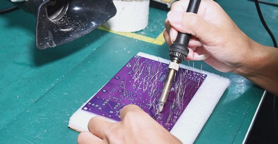
PCB Board Drawing Technology Guide
- Use network labels (NET) instead of text labels (TEXT) when creating the schematic diagram to avoid issues during PCB design guidance.
- Ensure all components in the schematic are properly packaged for recognition during PCB guidance. Create manual components if necessary to build a personal library for convenience.
- After drawing components, rename them sequentially and annotate them in order using the TOOLS menu.
- Generate a netlist report before converting to PCB by selecting “Create Netlist” from the DESIGN menu.
- Check electrical rules by navigating to TOOLS and selecting ERC.
- Focus on a well-planned layout with short traces and minimal vias for the PCB design.
- Prior to routing, set design rules for trace width, vias, and clearance constraints in the TOOLS menu.
- Optimize trace width for different types of traces and avoid right-angle turns for better signal integrity.
- Mark power, ground, and critical signals on the top layer for easier connection debugging.
- Choose between inches or millimeters in the VIEW menu for measurement units.
- Apply copper plating to enhance the board’s resistance to interference by selecting the copper-plated icon and configuring the copper coating options.
If you require PCB manufacturing services, feel free to contact me.
For the latest trends and updates in PCB technology, visit Well Circuits PCB Fabrication.