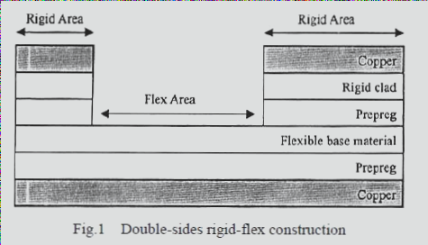
Designing Rigid-Flex Boards and Finding Circuit Board Processing Services in China
When designing rigid-flex boards, special software and specifications are often required. Flexible printed circuits (FPCs) can be designed using general PCB design software and are typically produced in Gerber format by FPC manufacturers. Manufacturers may have limitations on minimum line width, spacing, and vias. Adding copper layers to reinforce turning points can enhance durability. To find circuit board processing services in China, search online using “FPC” as a keyword.
Selecting Grounding Points Between PCB and Enclosure
The selection of grounding points between the PCB and the enclosure should prioritize utilizing chassis ground to create a low-impedance path for return currents. Connecting the PCB’s ground layer to the chassis ground near high-frequency devices reduces electromagnetic radiation by minimizing the current loop area.
Starting Circuit Board Debugging
When debugging a circuit board, begin by confirming power supply values, clock signal frequencies, and reset signal compliance. Ensure the chip outputs the first cycle signal and debug based on system principles and bus protocols.
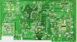
Techniques for High-Speed, High-Density PCB Design
In high-speed, high-density PCB design, manage crosstalk interference by maintaining trace continuity, considering trace spacing, selecting termination methods, and avoiding overlapping trace directions. Use blind or buried vias and differential termination to enhance signal integrity.
Effectiveness of LC Filtering Compared to RC Filtering
LC filtering for analog power supplies may be less effective than RC filtering if the inductor value and frequency band are not suitable. RC filtering can lead to energy loss and lower efficiency due to resistor power consumption, so resistor power rating should be considered.
PCB Design Considerations for Minimizing Electromagnetic Interference
- When designing PCBs, it is crucial to consider the inductor value not only based on the target noise frequency but also on the instantaneous current response capability. High inductance values can impede current flow and increase ripple noise, especially if the LC output terminal produces large instantaneous currents.
- The capacitor value is directly related to the acceptable ripple noise specification. Lower ripple noise requirements demand larger capacitance values. The ESR/ESL characteristics of the capacitor also impact its performance.
- When integrating an LC circuit at the output of a switching regulator, it is essential to evaluate the poles and zeros generated by the LC on the stability of the negative feedback control loop.
Meeting EMC Requirements on PCBs
Meeting EMC requirements on PCBs without incurring excessive costs can be challenging. Additional ground layers for improved shielding and the inclusion of ferrite beads, chokes, and other high-frequency suppression devices often contribute to increased costs associated with EMC compliance.
Coordinating shielding structures with other components is necessary to ensure the entire system meets EMC standards.
PCB Design Techniques to Reduce Electromagnetic Radiation
- Choose devices with slower signal slew rates to minimize high-frequency components generated by signals.
- Avoid placing high-frequency components too close to external connectors.
- Ensure proper impedance matching for high-speed signals and their return current paths to reduce high-frequency reflections and radiation.
- Install adequate decoupling capacitors on power supply pins of devices to decrease noise on power and ground planes, considering frequency response and temperature characteristics.
- Isolate the ground near external connectors and connect the connector ground to a nearby chassis ground.
- Implement ground guard or shunt traces alongside specific high-speed signals as needed, while monitoring the impact on trace impedance.
- Position the power layer at a distance of 20H from the ground layer, where H represents the separation between the power and ground planes.
Digital and Analog Ground Separation in PCBs
The practice of segregating digital and analog grounds in PCBs is conventional due to the noise generated by digital circuits during high-to-low potential transitions. Noise levels are influenced by signal speed and current levels. Failure to separate digital and analog grounds can result in significant noise interference from digital circuits affecting analog components, even if their signal paths do not intersect. Separation is essential unless the analog area is sufficiently isolated from the high-noise digital section.