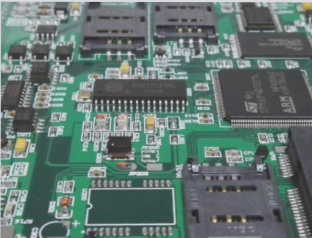
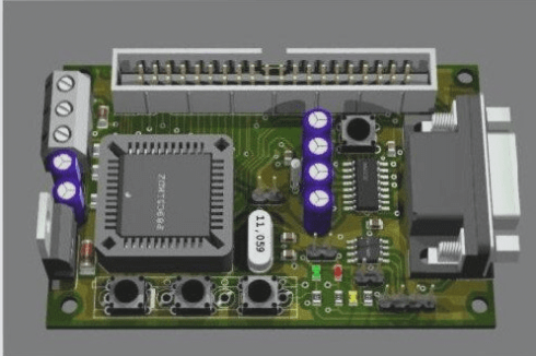
In the process of PCB circuit board production, soldering is an essential and critical step. After the soldering process, it is sometimes observed that white residues appear on the circuit board. These residues not only affect the aesthetic appearance of the board but may also impact its performance. Therefore, it is important to identify the causes of these white residues and address them accordingly.
**Causes and Solutions for White Residue After PCB Soldering:**
1. White residues typically result from improper flux usage. Rosin-based fluxes, in particular, tend to leave white spots during cleaning. Switching to different types of flux may prevent this issue in some cases.
2. Residues on the circuit board during production can lead to white spots after extended storage. A strong solvent can be used to clean the board and remove these residues.
3. Incorrect handling of circuit boards can also cause white spots. Often, a specific batch of circuit boards will exhibit this issue while others do not. In such cases, cleaning with a strong solvent can help resolve the problem.
4. The flux may be incompatible with the oxidation process. Switching to a different flux can help resolve this issue and improve the overall outcome.
5. Solvents used during the manufacturing process can degrade the PCB materials, resulting in white residues. To minimize this, it is important to reduce storage time. The nickel plating process, in particular, is known to cause this issue and requires careful attention.
6. Over time, flux can age and absorb moisture from the air, leading to the formation of white spots. Using fresh flux and cleaning the solder joints promptly after soldering can prevent this problem.
If white residue appears after the PCB is soldered, it should be addressed promptly. By analyzing the cause and applying the appropriate solution, the circuit board can maintain both its performance and appearance.
**Summary of Practical Skills in High-Frequency PCB Design**

1. The goal of PCB design is to create smaller, faster, and more cost-effective solutions. Since the interconnection point is the most vulnerable part of the circuit chain, the electromagnetic characteristics at these points represent the primary challenges in RF design. Every interconnection point must be thoroughly analyzed, and any potential issues should be addressed. The interconnection of a PCB system includes three main types: the chip-to-board connection, the interconnections within the PCB, and the signal I/O between the PCB and external devices. This article provides an overview of practical techniques for high-frequency PCB design, focusing on interconnections within the PCB. Understanding these techniques will be beneficial for future PCB design projects.
2. In PCB design, the chip-to-board interconnection plays a critical role. However, the main issue with these interconnections is the high density, which can lead to limitations in the basic structure of the PCB material. This can, in turn, restrict the overall growth of interconnection density. This article offers practical tips for high-frequency PCB design, specifically for interconnections within the PCB. For high-frequency applications, the following design techniques should be considered:
3. Transmission line corners should be designed with a 45° angle to reduce return loss.
4. Use high-performance dielectric circuit boards, where the dielectric constant is strictly controlled based on the number of layers. This approach aids in the accurate simulation of the electromagnetic field between the insulating material and the adjacent traces.
5. PCB design specifications for high-precision etching must be carefully defined. It’s essential to account for a total tolerance of +/-0.0007 inches for line width, properly manage the undercut and cross-section of trace shapes, and specify the plating conditions for the trace sidewalls. Effective management of trace geometry and surface coatings is crucial to addressing the skin effect at microwave frequencies and meeting these design standards.
6. Protruding pin leads introduce tap inductance and parasitic effects. Therefore, it’s best to avoid components with leads in high-frequency environments. Surface-mount (SMD) components should be used instead.
7. For PCB signal vias, avoid using the through-hole process (PTH) on sensitive areas of the PCB. This process can introduce inductance at the vias. For example, a through-hole on a 20-layer PCB that connects layers 1 to 3 will have inductance from layers 4 to 19, making buried or blind vias, or back drilling, a better solution.
8. Provide a continuous and solid ground plane. Use molded holes to connect these ground planes, ensuring that the 3D electromagnetic field doesn’t negatively impact the circuit.
9. Choose electroless nickel or immersion gold plating processes, and avoid using the HASL (Hot Air Solder Leveling) process for electroplating. The surface produced by these methods offers better skin effect characteristics for high-frequency currents. Additionally, these coatings are highly solderable, reduce the number of PCB leads, and contribute to reducing environmental pollution.
10. While solder masks help prevent solder paste flow, covering the entire board with a solder mask can alter circuit performance in microstrip designs. This happens due to variations in mask thickness and the dielectric constant. Typically, a solder dam is used as a solder mask to minimize these effects.
If you have any PCB manufacturing needs, please do not hesitate to contact me.Contact me
**Causes and Solutions for White Residue After PCB Soldering:**
1. White residues typically result from improper flux usage. Rosin-based fluxes, in particular, tend to leave white spots during cleaning. Switching to different types of flux may prevent this issue in some cases.
2. Residues on the circuit board during production can lead to white spots after extended storage. A strong solvent can be used to clean the board and remove these residues.
3. Incorrect handling of circuit boards can also cause white spots. Often, a specific batch of circuit boards will exhibit this issue while others do not. In such cases, cleaning with a strong solvent can help resolve the problem.
4. The flux may be incompatible with the oxidation process. Switching to a different flux can help resolve this issue and improve the overall outcome.
5. Solvents used during the manufacturing process can degrade the PCB materials, resulting in white residues. To minimize this, it is important to reduce storage time. The nickel plating process, in particular, is known to cause this issue and requires careful attention.
6. Over time, flux can age and absorb moisture from the air, leading to the formation of white spots. Using fresh flux and cleaning the solder joints promptly after soldering can prevent this problem.
If white residue appears after the PCB is soldered, it should be addressed promptly. By analyzing the cause and applying the appropriate solution, the circuit board can maintain both its performance and appearance.
**Summary of Practical Skills in High-Frequency PCB Design**

1. The goal of PCB design is to create smaller, faster, and more cost-effective solutions. Since the interconnection point is the most vulnerable part of the circuit chain, the electromagnetic characteristics at these points represent the primary challenges in RF design. Every interconnection point must be thoroughly analyzed, and any potential issues should be addressed. The interconnection of a PCB system includes three main types: the chip-to-board connection, the interconnections within the PCB, and the signal I/O between the PCB and external devices. This article provides an overview of practical techniques for high-frequency PCB design, focusing on interconnections within the PCB. Understanding these techniques will be beneficial for future PCB design projects.
2. In PCB design, the chip-to-board interconnection plays a critical role. However, the main issue with these interconnections is the high density, which can lead to limitations in the basic structure of the PCB material. This can, in turn, restrict the overall growth of interconnection density. This article offers practical tips for high-frequency PCB design, specifically for interconnections within the PCB. For high-frequency applications, the following design techniques should be considered:
3. Transmission line corners should be designed with a 45° angle to reduce return loss.
4. Use high-performance dielectric circuit boards, where the dielectric constant is strictly controlled based on the number of layers. This approach aids in the accurate simulation of the electromagnetic field between the insulating material and the adjacent traces.
5. PCB design specifications for high-precision etching must be carefully defined. It’s essential to account for a total tolerance of +/-0.0007 inches for line width, properly manage the undercut and cross-section of trace shapes, and specify the plating conditions for the trace sidewalls. Effective management of trace geometry and surface coatings is crucial to addressing the skin effect at microwave frequencies and meeting these design standards.
6. Protruding pin leads introduce tap inductance and parasitic effects. Therefore, it’s best to avoid components with leads in high-frequency environments. Surface-mount (SMD) components should be used instead.
7. For PCB signal vias, avoid using the through-hole process (PTH) on sensitive areas of the PCB. This process can introduce inductance at the vias. For example, a through-hole on a 20-layer PCB that connects layers 1 to 3 will have inductance from layers 4 to 19, making buried or blind vias, or back drilling, a better solution.
8. Provide a continuous and solid ground plane. Use molded holes to connect these ground planes, ensuring that the 3D electromagnetic field doesn’t negatively impact the circuit.
9. Choose electroless nickel or immersion gold plating processes, and avoid using the HASL (Hot Air Solder Leveling) process for electroplating. The surface produced by these methods offers better skin effect characteristics for high-frequency currents. Additionally, these coatings are highly solderable, reduce the number of PCB leads, and contribute to reducing environmental pollution.
10. While solder masks help prevent solder paste flow, covering the entire board with a solder mask can alter circuit performance in microstrip designs. This happens due to variations in mask thickness and the dielectric constant. Typically, a solder dam is used as a solder mask to minimize these effects.
If you have any PCB manufacturing needs, please do not hesitate to contact me.Contact me


