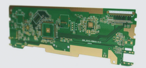
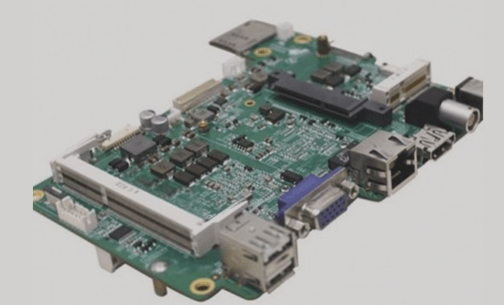
The general surface treatments for PCB circuit boards include tin spraying, OSP, and gold immersion. The term “surface” here refers to the connection points on the PCB that establish electrical connections between electronic components or other systems and the PCB’s circuitry, such as the pad or contact points. While bare copper itself has excellent solderability, it is prone to oxidation and contamination when exposed to air, which is why surface treatment is essential for PCBs.
1. **Tin Spraying (HASL)**
For applications dominated by through-hole devices, wave soldering is the preferred soldering method. Hot-Air Solder Leveling (HASL) surface treatment technology is typically sufficient to meet the process requirements for wave soldering. However, for applications that require higher joint strength, particularly in contact connections, nickel/gold electroplating is commonly used. HASL remains the dominant surface treatment technology worldwide. That said, three key factors—cost, evolving process requirements, and the shift to lead-free soldering—are driving the electronics industry to explore alternatives to HASL.

1. **Cost Considerations**
From a cost perspective, many electronic components, such as those used in mobile communications and personal computers, are increasingly becoming consumer products. In today’s highly competitive market, the only way to remain invincible is to sell at cost or lower prices. With the development of assembly technologies like Surface-Mount Technology (SMT), PCB pads now require screen printing and reflow soldering during the assembly process. In the case of SMA, the PCB surface treatment initially relied on HASL (Hot Air Solder Leveling) technology. However, as SMT devices continue to shrink, pad and stencil openings have also become smaller, exposing the limitations of HASL. Pads treated with HASL are not sufficiently flat, and the coplanarity does not meet the requirements of fine-pitch pads. Environmental concerns are often focused on the potential lead contamination from HASL and its impact on the environment.
2. **Organic Solderability Protective Layer (OSP)**
Organic Solderability Preservative (OSP) is an organic coating used to protect copper from oxidation before soldering, thereby preserving the solderability of PCB pads.
After the PCB surface is treated with OSP, a thin organic layer forms on the copper to prevent oxidation. For example, Benzotriazole-based OSP typically has a thickness of 100 Å, while Imidazole-based OSP is thicker, usually around 400 Å. OSP is transparent, which makes it difficult to detect by eye. During assembly (reflow soldering), the OSP layer melts into the solder paste or acidic flux, exposing the active copper surface, which then forms Sn/Cu intermetallic compounds between the components and the pads. This makes OSP an excellent solution for treating soldering surfaces. Additionally, OSP does not contribute to lead pollution, making it environmentally friendly.
**Limitations of OSP:**
1. OSP’s transparent nature makes it difficult to inspect, and distinguishing whether a PCB has been treated with OSP can be challenging.
2. Since OSP itself is an insulator, it does not conduct electricity. The thin OSP layer in Benzotriazoles typically does not affect electrical testing, but the thicker Imidazole-based OSP may interfere with electrical tests. OSP should not be used for electrical contact surfaces, such as key surfaces in keyboards.
3. Stronger flux is required during the soldering process to eliminate the protective OSP layer; otherwise, soldering defects may occur.
4. During storage, OSP-treated surfaces should be kept away from acidic substances and excessive temperatures, as these conditions may cause the OSP to volatilize.
3. **Immersion Gold (ENIG)**
**Protection Mechanism of ENIG:**
Immersion Gold (ENIG) involves chemically plating a Ni/Au layer onto the copper surface. The typical nickel thickness ranges from 120 to 240 μin (about 3 to 6 μm), while the gold layer is thinner, usually between 2 to 4 μin (0.05 to 0.1 μm). Nickel serves as a barrier between the solder and copper. During soldering, the gold layer quickly melts into the solder, and the solder forms a Ni/Sn intermetallic compound with the nickel. The gold layer prevents the oxidation or passivation of the nickel during storage, which is why it is important for the gold layer to be sufficiently dense and not too thin.
**Immersion Gold Process:**
The goal of the immersion gold process is to deposit a thin, continuous gold layer. The gold layer should not be too thick, as this could make solder joints brittle, negatively impacting the reliability of the solder connections. Like nickel plating, immersion gold can withstand high temperatures and extended exposure times. During the process, a displacement reaction occurs where gold replaces nickel on the copper surface. Once the displacement reaction reaches a certain level, it automatically stops. Gold’s high strength, wear resistance, and excellent oxidation resistance make it ideal for protecting nickel, especially in high-stress applications.
PCBs treated with ENIG are very flat with excellent coplanarity, making it the preferred choice for button contact surfaces. Furthermore, ENIG provides excellent solderability, as gold quickly melts into the molten solder, exposing fresh nickel beneath.
**Limitations of ENIG:**
The ENIG process is relatively complex, and achieving optimal results requires strict control over the process parameters. A significant challenge is that ENIG-treated PCB surfaces are prone to the formation of “black pads” during ENIG processing or soldering. This issue can severely impact the reliability of solder joints. The mechanism behind black pad formation is complex and occurs at the interface between nickel and gold, typically caused by excessive oxidation of the nickel. Additionally, excessive gold plating can embrittle the solder joints, reducing their overall reliability.
1. **Tin Spraying (HASL)**
For applications dominated by through-hole devices, wave soldering is the preferred soldering method. Hot-Air Solder Leveling (HASL) surface treatment technology is typically sufficient to meet the process requirements for wave soldering. However, for applications that require higher joint strength, particularly in contact connections, nickel/gold electroplating is commonly used. HASL remains the dominant surface treatment technology worldwide. That said, three key factors—cost, evolving process requirements, and the shift to lead-free soldering—are driving the electronics industry to explore alternatives to HASL.

1. **Cost Considerations**
From a cost perspective, many electronic components, such as those used in mobile communications and personal computers, are increasingly becoming consumer products. In today’s highly competitive market, the only way to remain invincible is to sell at cost or lower prices. With the development of assembly technologies like Surface-Mount Technology (SMT), PCB pads now require screen printing and reflow soldering during the assembly process. In the case of SMA, the PCB surface treatment initially relied on HASL (Hot Air Solder Leveling) technology. However, as SMT devices continue to shrink, pad and stencil openings have also become smaller, exposing the limitations of HASL. Pads treated with HASL are not sufficiently flat, and the coplanarity does not meet the requirements of fine-pitch pads. Environmental concerns are often focused on the potential lead contamination from HASL and its impact on the environment.
2. **Organic Solderability Protective Layer (OSP)**
Organic Solderability Preservative (OSP) is an organic coating used to protect copper from oxidation before soldering, thereby preserving the solderability of PCB pads.
After the PCB surface is treated with OSP, a thin organic layer forms on the copper to prevent oxidation. For example, Benzotriazole-based OSP typically has a thickness of 100 Å, while Imidazole-based OSP is thicker, usually around 400 Å. OSP is transparent, which makes it difficult to detect by eye. During assembly (reflow soldering), the OSP layer melts into the solder paste or acidic flux, exposing the active copper surface, which then forms Sn/Cu intermetallic compounds between the components and the pads. This makes OSP an excellent solution for treating soldering surfaces. Additionally, OSP does not contribute to lead pollution, making it environmentally friendly.
**Limitations of OSP:**
1. OSP’s transparent nature makes it difficult to inspect, and distinguishing whether a PCB has been treated with OSP can be challenging.
2. Since OSP itself is an insulator, it does not conduct electricity. The thin OSP layer in Benzotriazoles typically does not affect electrical testing, but the thicker Imidazole-based OSP may interfere with electrical tests. OSP should not be used for electrical contact surfaces, such as key surfaces in keyboards.
3. Stronger flux is required during the soldering process to eliminate the protective OSP layer; otherwise, soldering defects may occur.
4. During storage, OSP-treated surfaces should be kept away from acidic substances and excessive temperatures, as these conditions may cause the OSP to volatilize.
3. **Immersion Gold (ENIG)**
**Protection Mechanism of ENIG:**
Immersion Gold (ENIG) involves chemically plating a Ni/Au layer onto the copper surface. The typical nickel thickness ranges from 120 to 240 μin (about 3 to 6 μm), while the gold layer is thinner, usually between 2 to 4 μin (0.05 to 0.1 μm). Nickel serves as a barrier between the solder and copper. During soldering, the gold layer quickly melts into the solder, and the solder forms a Ni/Sn intermetallic compound with the nickel. The gold layer prevents the oxidation or passivation of the nickel during storage, which is why it is important for the gold layer to be sufficiently dense and not too thin.
**Immersion Gold Process:**
The goal of the immersion gold process is to deposit a thin, continuous gold layer. The gold layer should not be too thick, as this could make solder joints brittle, negatively impacting the reliability of the solder connections. Like nickel plating, immersion gold can withstand high temperatures and extended exposure times. During the process, a displacement reaction occurs where gold replaces nickel on the copper surface. Once the displacement reaction reaches a certain level, it automatically stops. Gold’s high strength, wear resistance, and excellent oxidation resistance make it ideal for protecting nickel, especially in high-stress applications.
PCBs treated with ENIG are very flat with excellent coplanarity, making it the preferred choice for button contact surfaces. Furthermore, ENIG provides excellent solderability, as gold quickly melts into the molten solder, exposing fresh nickel beneath.
**Limitations of ENIG:**
The ENIG process is relatively complex, and achieving optimal results requires strict control over the process parameters. A significant challenge is that ENIG-treated PCB surfaces are prone to the formation of “black pads” during ENIG processing or soldering. This issue can severely impact the reliability of solder joints. The mechanism behind black pad formation is complex and occurs at the interface between nickel and gold, typically caused by excessive oxidation of the nickel. Additionally, excessive gold plating can embrittle the solder joints, reducing their overall reliability.


