Environmental Sustainability in PCB Manufacturing
As the focus on environmental sustainability grows, issues related to PCB (Printed Circuit Board) manufacturing have come to the forefront. Lead and bromine usage are key concerns in the industry, leading to discussions about transitioning to lead-free and halogen-free PCBs. This shift is expected to have a significant impact on future technological advancements.
Importance of Surface Treatment
The main goal of surface treatment in PCB manufacturing is to ensure optimal solderability and reliable electrical performance. Copper, the primary conductive material in PCBs, quickly forms oxide layers when exposed to air, hindering soldering and electrical connectivity. Surface treatments are essential to maintain the integrity of copper and prevent these issues.
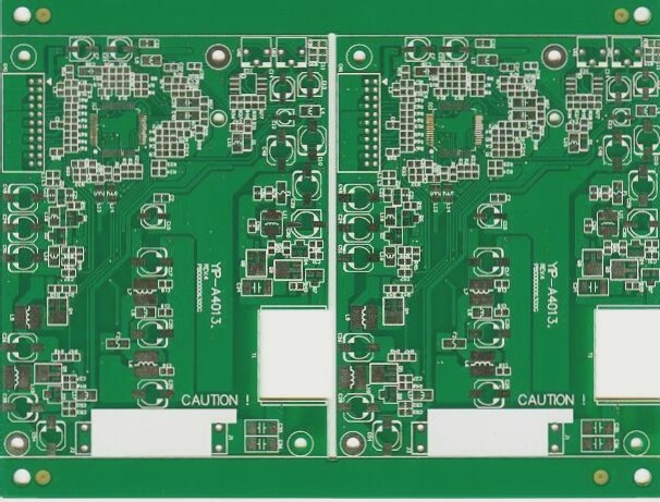
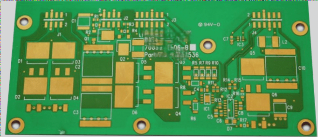
Common Surface Treatment Processes for PCBs
Various surface treatment processes are utilized in PCB production, each offering specific benefits based on the application. The five most common processes include Hot Air Leveling (HAL), Organic Coating (OC), Electroless Nickel/Immersion Gold (ENIG), Immersion Silver, and Immersion Tin. Here’s an overview of each process:
Hot Air Leveling (HAL)
Hot Air Leveling, also known as Hot Air Solder Leveling (HASL), involves applying molten tin-lead solder to the PCB surface. Compressed air is then used to flatten the solder, creating a uniform protective coating that resists copper oxidation and enhances solderability. The process forms a copper-tin intermetallic compound to protect against oxidation and typically results in a solder thickness of 1-2 mils.
Organic Coating (OC)
Organic Coating acts as a barrier between copper traces and air, preventing oxidation. This cost-effective process utilizes molecules like benzimidazole to chemically bond nitrogen functional groups to the copper surface, providing durable protection. Multiple layers of organic coating ensure longevity and excellent performance during lead-free soldering operations.
Advantages of Different PCB Surface Treatments
-
Organic Coating
Organic Coating is known for its simple process control, making it a popular choice for surface treatment. It acts as an anti-rust barrier, providing basic protection for PCBs.
-
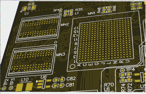
Electroless Nickel/Immersion Gold (ENIG)
ENIG is a complex process used for multilayer PCBs. It involves applying a layer of electroless nickel followed by a thin immersion gold layer. This treatment offers superior electrical properties, mechanical strength, and oxidation resistance.
-
Immersion Silver
Immersion Silver is favored for its excellent solderability and environmental friendliness. It provides good electrical conductivity and is ideal for lead-free soldering applications.
-
Immersion Tin
Immersion Tin offers good solderability at a lower cost. While it may degrade over time, it remains a suitable option for budget-sensitive applications.
Manufacturers choose surface treatments based on factors like solderability, durability, and cost to optimize PCB production.