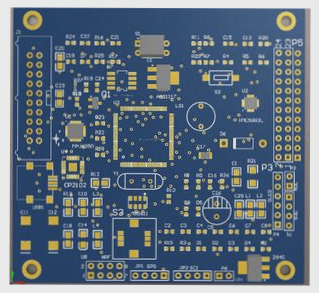
Ten Common Defects in PCB Design Process
The processing level definition is unclear, leading to potential mounting issues; excessive copper foil proximity to the outer frame risks warping; pads with filling blocks may pass design checks but fail in manufacturing; flower pad connections must avoid gaps; misaligned character pads complicate testing; short pads hinder probe alignment; single-sided pad apertures must be set correctly; overlapping pads can damage holes; excessive filling blocks complicate optical data; and misuse of graphic layers results in confusion, violating design standards.

